Optical metrology of periodic targets in presence of multiple diffraction orders

a technology of diffraction order and optical metrology, which is applied in the direction of semiconductor/solid-state device testing/measurement, instruments, photomechanical equipment, etc., can solve the problem of insufficient ability to calculate separate diffraction orders to accurately or reliably fit measured data, and more interference terms in the reflected signal

Active Publication Date: 2016-01-26
KLA TENCOR TECH CORP
View PDF21 Cites 26 Cited by
  • Summary
  • Abstract
  • Description
  • Claims
  • Application Information

AI Technical Summary

Benefits of technology

[0007]In one embodiment, a method of obtaining optical signal measurements from a periodic semiconductor target is disclosed. The method includes selecting one or more zero or non-zero diffraction orders for eliminating or obtaining corresponding non-zero diffraction order terms or interference term from a plurality of measurements from a periodic target using an optical metrology tool. The periodic target has a pitch, and the plurality of measurements contain a zero diffraction order term and one or more non-zero diffraction order terms. Using the optical metrology tool, an incident beam is directed to a plurality of positions on the target, and the measurements are obtained from the target in response to the incident beam being directed to each position. The measurements from the positions of the targets are processed to eliminate or obtain each zero or non-zero diffraction order term or interference term associated with each selected zero or non-zero diffraction order, resulting in a processed metrology signal. The positions are shifted from each other so as to cause the zero or non-zero diffraction order term or interference term corresponding to each selected zero or non-zero diffraction order to be eliminated or obtained.
[0008]In a specific implementation, the processed metrology signal is used in a model-based metrology process for determining one or more parameters of the target. In another implementation, the processed metrology signal is used in a calibration process for the optical metrology tool. In one aspect, one or more non-zero diffraction orders are selected and the measurements are processed so that the processed metrology signal retains only zero diffraction terms and eliminates non-zero diffraction order terms corresponding to the selected one or more non-zero diffraction orders. In another aspect, one or more non-zero diffraction orders are selected and the measurements are processed so that the processed metrology signal retains only zero diffraction terms and separated one or more non-zero diffraction order terms corresponding to the selected one or more non-zero diffraction orders, while eliminating interference terms corresponding to the selected one or more non-zero diffraction orders. The measurements are electric field measurements, and the measurements are processed so that the processed metrology signal is equal to an average of the electric field measurements from the positions. In one aspect, the electric field measurements are obtained in the near-field portion of the optical metrology system. In another aspect, the electric field measurements are obtained in the far-field portion of the optical metrology system. In another implementation, the measurements are intensity measurements, and the measurements are processed so that the processed metrology signal is equal to an average of the intensity measurements from the positions.
[0009]In another embodiment, each relative shift between the positions is selected based on the selected one or more non-zero diffraction orders, while an absolute value for each position is unspecified. In one aspect, the positions are shifted with respect to each other by a rational fraction of the pitch based on the selected one or more non-zero diffraction orders. In a detailed example, the measurements include a spatial average of a plurality of sub-measurements for each position. In another example, the target comprises gratings arranged in two directions. In a specific implementation, the measurements are obtained using a plurality of incident beams directed simultaneously to at least two of the positions.
[0010]In one embodiment, the measurements are processed so that the processed metrology signal retains only zero diffraction terms and one or more non-zero diffraction order terms not corresponding to the selected one or more diffraction orders and eliminates non-zero diffraction order terms corresponding to the selected one or more diffraction orders. In one aspect, the measurements are processed so that the processed measurement signal retains an individual interference term corresponding to one of the selected one or more diffraction orders and such individual interference term is retained by comparing the plurality of measurements to each other.
[0011]In an alternative embodiment, the invention pertains to an apparatus for obtaining optical signal measurements from a periodic semiconductor target. The apparatus includes a measurement module for directing an incident beam towards a periodic target having a pitch and a detection module for obtaining measurements having multiple diffraction orders from the periodic target in response to the incident beam. The apparatus further comprises a processor that is configured to perform one or more of the above described method operations.
[0012]These and other features of the present invention will be presented in more detail in the following specification of embodiments of the invention and the accompanying figures which illustrate by way of example the principles of the invention.

Problems solved by technology

For example, using multiple angles of incidence for particular wavelength ranges, e.g., lower wavelengths, may tend to cause more interference terms in the reflected signal.
However, there are several challenges in performing such model-to-data fitting in the presence of multiple diffraction orders.
For instance, larger pitch gratings tend to result in greater position dependent sensitivity.
Although goal is to fit the detected data to the output of the model so as to determine the characteristics of the grating under test, the ability to calculate separate diffraction orders is not sufficient to accurately or reliably fit measured data due to the challenges of interference, position dependence, and normalization.
That is, an RCWA technique does not account for interference terms in detected data and cannot be used with detected data having multiple interfering orders.
Since accurately measuring grating position tends to be difficult, it is also difficult to account for such position in an FEM data-fitting process in the presence of multiple diffraction orders.
The difference in the measured signal for different locations on a grating can also hinder calibration of the metrology tool when measurements include multiple diffraction orders that cause complex interference issues.
An increase in the measurement accuracy entails an increase in the complexity of the stage movement and coordinate system mechanism of the metrology tool.
Such accuracy may be impractical in some metrology systems.
However such a grating removes the zero order and all other orders, thereby, significantly reducing the amount of useful information.
This type of grating is also not very practical for semiconductor metrology, in which grating design is guided primarily by semiconductor device fabrication design rules
This deviation is caused by 1st order diffraction interference.
This placement technique would likely result in a higher incidence of defect capture and more reliable resulting products.

Method used


Image

  • Optical metrology of periodic targets in presence of multiple diffraction orders
  • Optical metrology of periodic targets in presence of multiple diffraction orders
  • Optical metrology of periodic targets in presence of multiple diffraction orders

Examples


Embodiment Construction

[0020]In the following description, numerous specific details are set forth in order to provide a thorough understanding of the present invention. The present invention may be practiced without some or all of these specific details. In other instances, well known component or process operations have not been described in detail to not unnecessarily obscure the present invention. While the invention will be described in conjunction with the specific embodiments, it will be understood that it is not intended to limit the invention to the embodiments.

INTRODUCTION

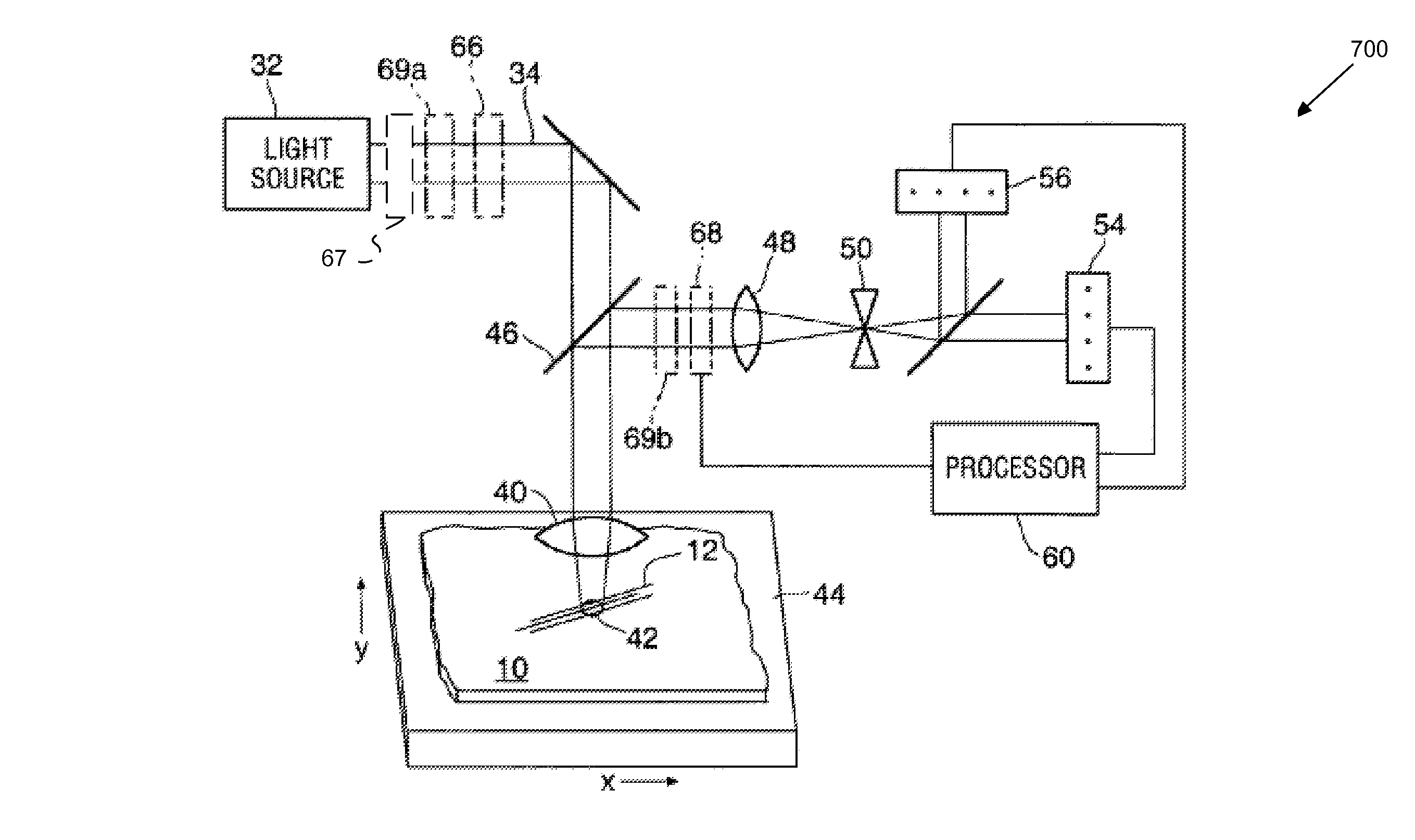
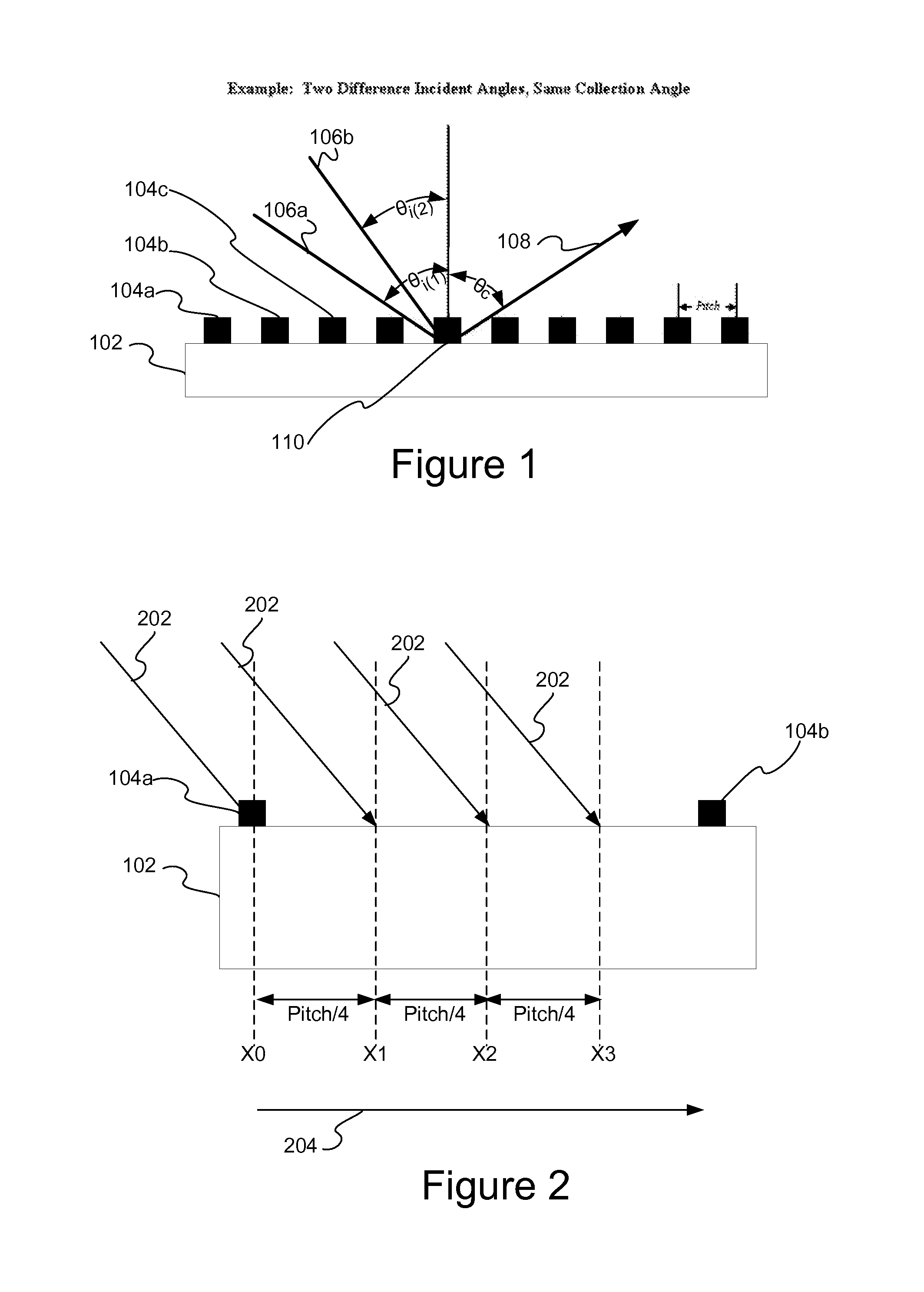
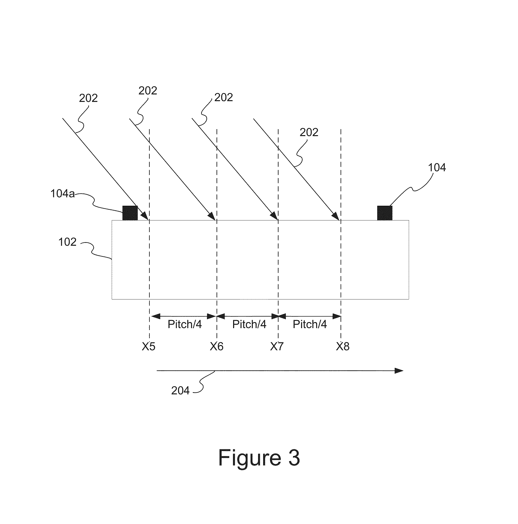
[0021]A beam profile reflectometry (BPR) example will first be described to illustrate challenges with processing optical signals having multiple diffraction order content. In a BPR system, a probe beam can be focused with a strong lens so that the rays within the probe beam strike a target at multiple angles of incidence. FIG. 1 illustrates a simplified BPR example having two rays of a probe beam at two different angles of inc...


PUM

PropertyMeasurementUnit
angles of incidenceaaaaaaaaaa
diameteraaaaaaaaaa
optical signalaaaaaaaaaa

Abstract

One or more non-zero diffraction orders are selected, and these selected one or more zero or non-zero diffraction orders are selected for eliminating or obtaining corresponding zero or non-zero diffraction order terms or interference term from measurements from a periodic target using an optical metrology tool. The periodic target has a pitch, and the measurements contain a zero diffraction order and one or more non-zero diffraction order terms. Using the optical metrology tool, an incident beam is directed to positions on the target, and the measurements are obtained from the target in response to the incident beam. The measurements are processed to eliminate or obtain each zero or non-zero diffraction order term or interference term associated with each selected zero or non-zero diffraction order, resulting in a processed metrology signal. The positions are shifted from each other so as to cause the zero or non-zero diffraction order term or interference term corresponding to each selected zero or non-zero diffraction order to be eliminated or obtained.

Description

CROSS-REFERENCE TO RELATED APPLICATIONS[0001]This application claims the benefit of U.S. Provisional Application No. 61 / 664,543, filed Jun. 26, 2012, by Alexander Kuznetsov et al., which application is herein incorporated by reference in its entirety for all purposes.BACKGROUND OF THE INVENTION[0002]The invention described herein relates generally to semiconductor metrology of a specimen, such as a wafer or reticle. More specifically, it relates to metrology that employs detection of an optical signal from a periodic target.[0003]Generally, the industry of semiconductor manufacturing involves highly complex techniques for fabricating integrated circuits using semiconductor materials which are layered and patterned onto a substrate, such as silicon. Due to the large scale of circuit integration and the decreasing size of semiconductor devices, the device must comply with rigorous specification requirements prior to shipment of the device to the end users or customers.[0004]Optical me...

Claims


Application Information

Patent Timeline
Patent Type & Authority Patents(United States)
IPC IPC(8): G01B9/02G01N21/47G01N21/956
CPCG01B9/02083G01N21/4788G01N21/956G01B2210/56G01N21/9501G01N21/95623G03F7/70625G01N21/4785H01L22/12
Inventor KUZNETSOV, ALEXANDERPETERLINZ, KEVINSHCHEGROV, ANDREI
Owner KLA TENCOR TECH CORP
Why Eureka
Try Eureka