Bond pad structure and method of manufacturing the same

a technology of bond pad and manufacturing method, which is applied in the direction of metallic pattern materials, solid-state devices, semiconductor/solid-state device details, etc., can solve the problems of lowering the possibility of bond pad damage during the etching process and lowering manufacturing costs, so as to reduce the possibility of bond pad damage during the etching process and reduce manufacturing costs

Active Publication Date: 2016-02-23
MARLIN SEMICON LTD
View PDF12 Cites 6 Cited by
  • Summary
  • Abstract
  • Description
  • Claims
  • Application Information

AI Technical Summary

Benefits of technology

[0008]To improve the above-mentioned drawbacks in the fabrication of the bond pad in prior art, a novel method of manufacturing a bond pad structure is provided in the present invention. A protection layer is used in present invention to cover the pad material layer before the pad material layer is etched and patterned into a bond pad. The protection layer is suitable for protecting the underlying pad material layer from corrosion or pad discoloration issue, thereby providing a larger process window for the bond pad loop. Moreover, the protection layer may be easily removed from the underlying bond pad structure by a simple strip or wet etching process after forming the bond pad, so this approach may lower the possibility of bond pad damage during the etching process and lower the manufacturing costs.

Problems solved by technology

Moreover, the protection layer may be easily removed from the underlying bond pad structure by a simple strip or wet etching process after forming the bond pad, so this approach may lower the possibility of bond pad damage during the etching process and lower the manufacturing costs.

Method used


Image

  • Bond pad structure and method of manufacturing the same
  • Bond pad structure and method of manufacturing the same
  • Bond pad structure and method of manufacturing the same

Examples


first embodiment

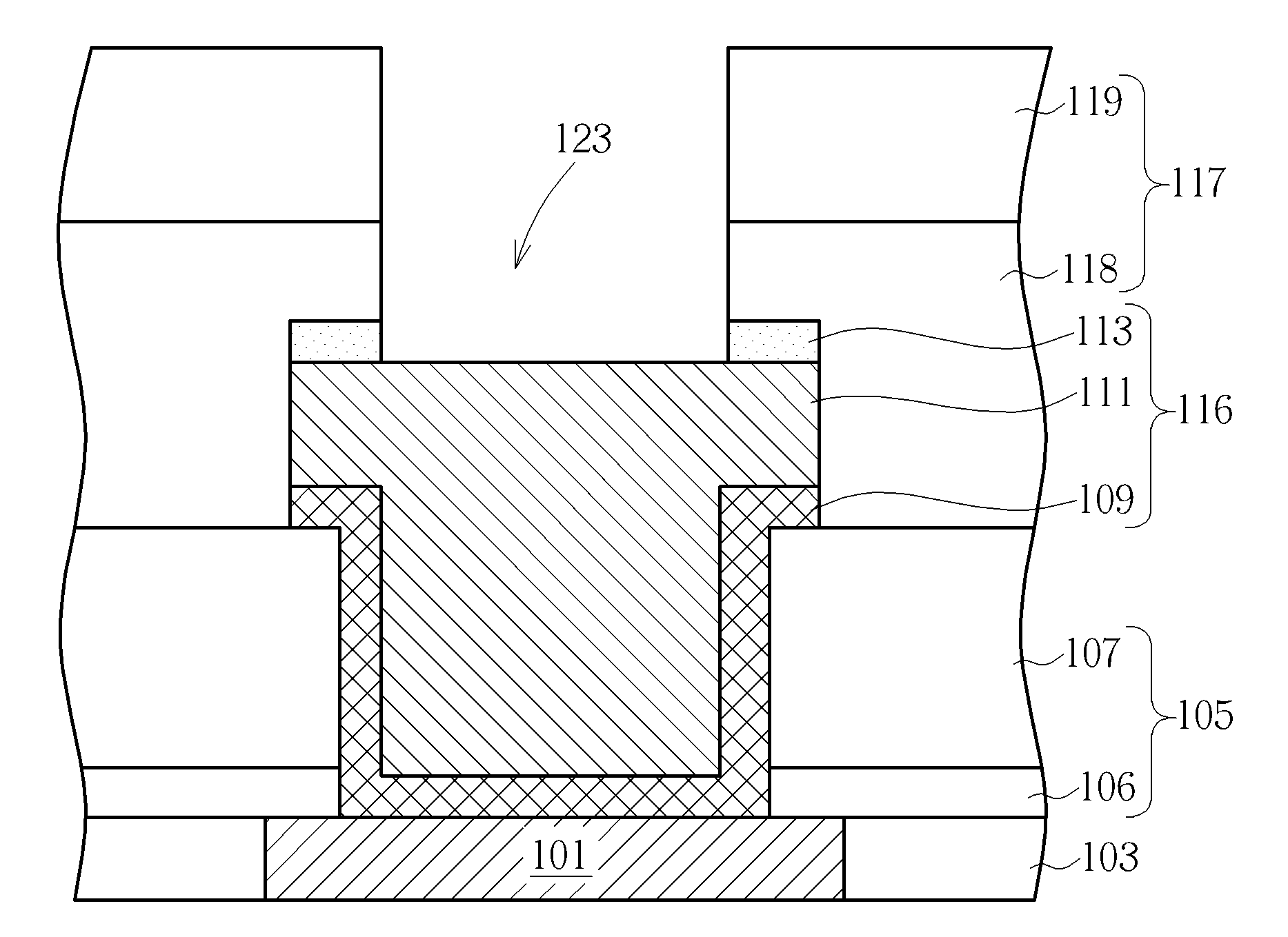
[0020]Please now refer to FIGS. 1-6, which illustrates the process flow in first embodiment of the present invention. The process of the present embodiment is particularly directed to form a protruding bond pad structure which is suitable for direct wire bonding in packaging processes.

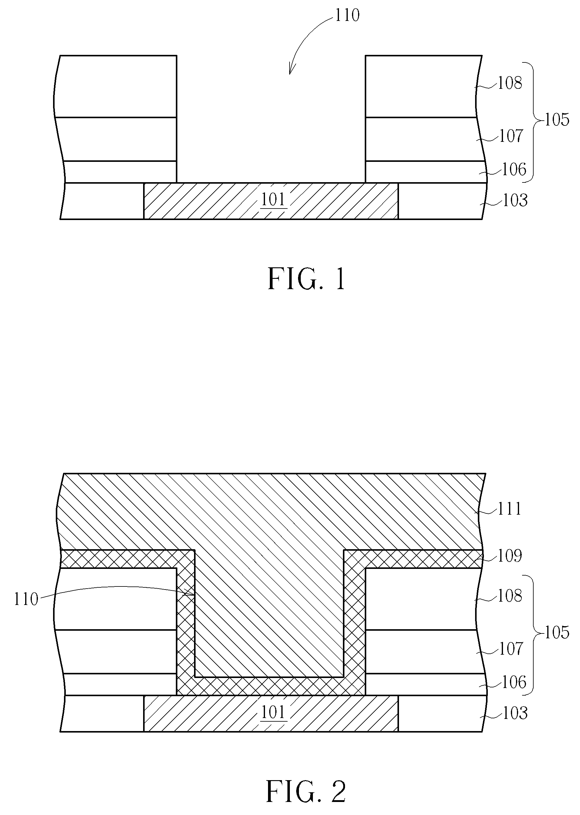
[0021]First, the process of present embodiment starts from a prepared copper interconnection, for example: a top metal Cu layer or a Cu contact. As shown in FIG.1, this copper structure may be a copper layer 101 deposited within a patterned opening formed in an insulating layer 103, such as a layer made of fluorinated TEOS (tetraethoxysilane) or fluorinated silicate glass (FSG). In the first place, the copper layer 101 is designed to serve as a contact for connecting the external electrical circuit. However, as mentioned in the description of the prior art, a copper interconnection may usually require an aluminum cap or pad structure to protect the copper from environmental deterioration, such as oxida...

second embodiment

[0030]Now, please refer to FIGS. 7-10 which illustrate the cross-sectional view of a process flow for manufacturing a bond pad structure with dual passivations in accordance with present invention.

[0031]The process of the present embodiment is particularly directed to form an embedded bond pad structure wherein each Al bond pad is embedded in, rather than protruding from the passivation layer. This kind of embedded bond may be suitable for processes or packaging with solder ball limiting metallurgy (BLM) or solder bumps.

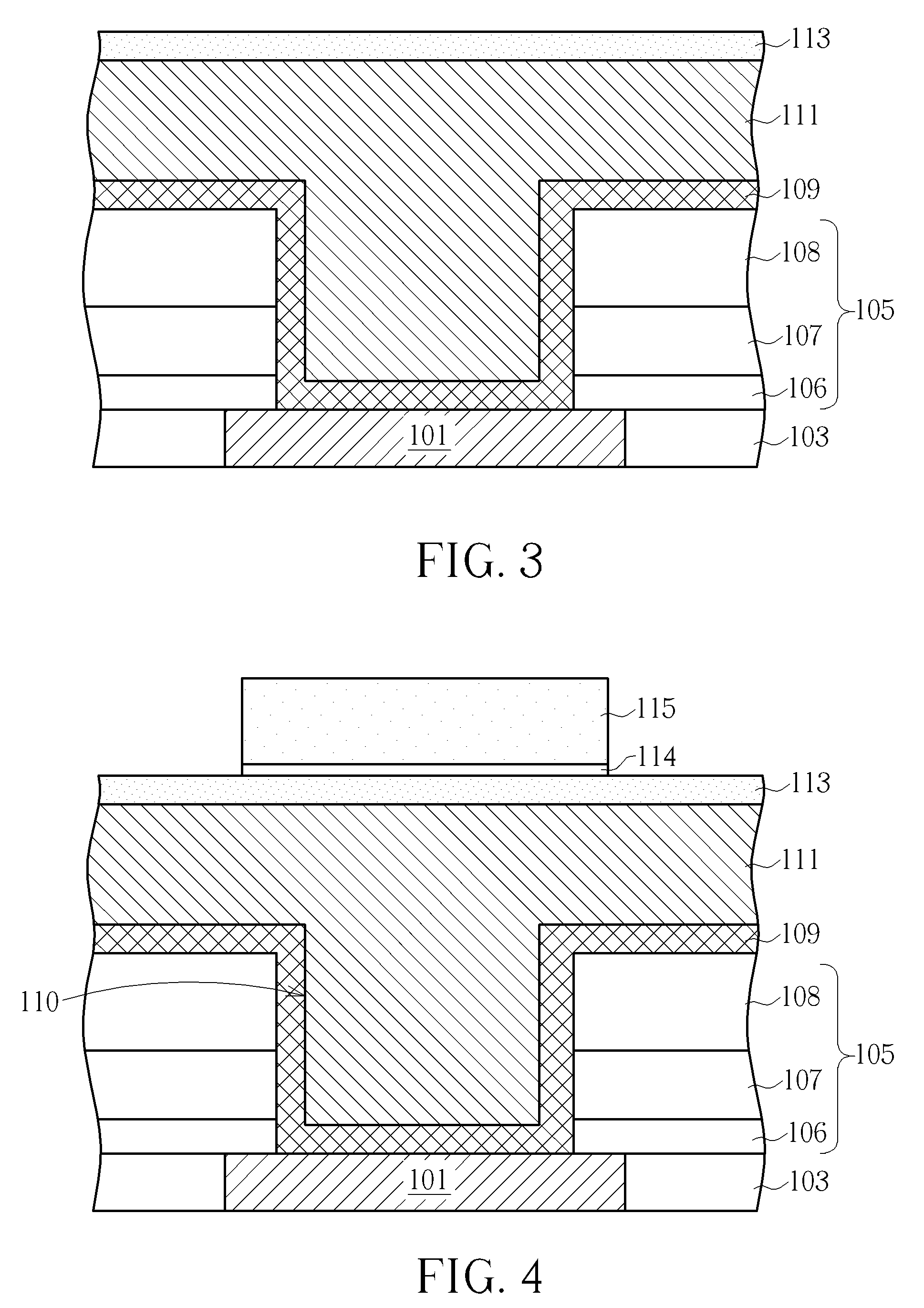
[0032]As shown in FIG. 7, the present embodiment starts from a prepared pad structure similar to the bond pad 116 shown in FIG. 5, wherein the protection layer 113 is still present on the bond pad structure, and the photoresist 115 and BARC 114 used in pad etching process have already been removed. The difference between the bond pad structures shown in FIG. 5 and FIG. 7 is that the passivation layer 105 of the bond pad structure in FIG. 7 is made of only a SiN layer...


PUM


Abstract

A method of manufacturing a bond pad structure, comprising the steps of forming a pad material layer on a passivation layer, forming a protection layer on the pad material layer, performing an etching process to pattern the protection layer and the pad material layer into a bond pad structure, and removing the protection layer on the bond pad structure.

Description

BACKGROUND OF THE INVENTION[0001]1. Field of the Invention[0002]The present invention generally relates to a method of manufacturing a bond pad structure and, more particularly, to a method of manufacturing a bond pad structure with a protection layer.[0003]2. Description of the Prior Art[0004]In semiconductor manufacturing, a fabricated integrated circuit (IC) device is typically assembled into a package to be utilized on a printed circuit board (such as a motherboard, etc) as part of a larger circuit. When the fabrication of the integrated circuit device (such as a die) is finished, the integrated circuit device is immovably bound and sealed using an electronic package technique so as to prevent damages from an external force or other environmental factors. A package substrate is often used in the electronic package industry to affix the integrated circuit device thereon, and it also provides one or more layers of metal interconnects, wherein one end of the metal interconnect is e...

Claims


Application Information

Patent Timeline
Patent Type & Authority Patents(United States)
IPC IPC(8): H05K1/03H05K1/09H05K3/22H01L23/31H01L23/00H05K1/02H01L21/44H01L21/28H01L23/48
CPCH01L24/05H01L23/3192H01L24/03H01L2224/03009H01L2224/0345H01L2224/0362H01L2224/0401H01L2224/04042H01L2224/05567H01L2224/05572H01L2924/00014H01L2924/00012H01L2224/05166H01L2224/05181H01L2224/05186H01L2224/131H01L2924/01074H01L2924/04941H01L2924/04953H01L2924/014H01L23/5226H01L23/528H01L23/53219H01L23/53223H01L23/53295H01L29/24
Inventor WANG, YE
Owner MARLIN SEMICON LTD
Why Eureka
Try Eureka