
Hole blocking layer and method for producing same, and photoelectric conversion element comprising the hole blocking layer and method for manufacturing same

a technology of photoelectric conversion element and hole blocking layer, which is applied in the direction of sustainable manufacturing/processing, final product manufacturing, nanoinformatics, etc., to achieve excellent hole blocking ability and light transmissivity, and high initial photoelectric conversion efficiency. , the effect of excellent durability

Active Publication Date: 2016-03-22
IDEAL STAR
View PDF9 Cites 1 Cited by
  • Summary
  • Abstract
  • Description
  • Claims
  • Application Information

AI Technical Summary

Benefits of technology

[0016]The characteristics of an organic thin-film solar cell-type photoelectric conversion element can be thus enhanced by interposing, between an electrode and an organic semiconductor, an interlayer that increases carrier transport efficiency. However, further improvements in the composition and structure of such an interlayer are required.
[0018]In the light of the above, it is an object of the present invention to provide a hole-blocking layer that has excellent basic characteristics such as high photoelectric conversion efficiency as well as excellent productivity, and to provide a method for producing the hole-blocking layer, and to provide as well a photoelectric conversion element, such as an organic thin-film solar cell and organic EL element, comprising the hole-blocking layer, and a method for producing the photoelectric conversion element.
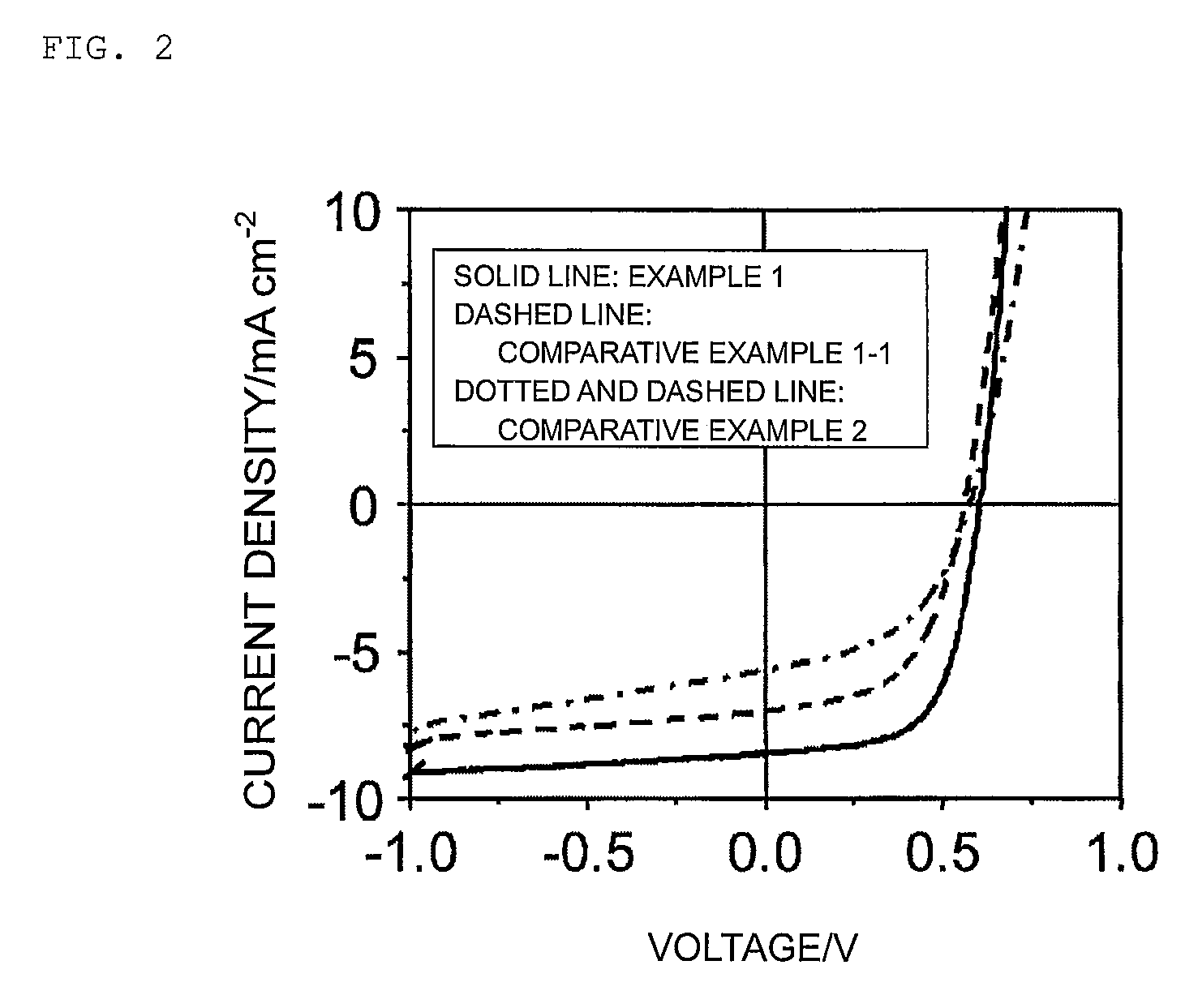
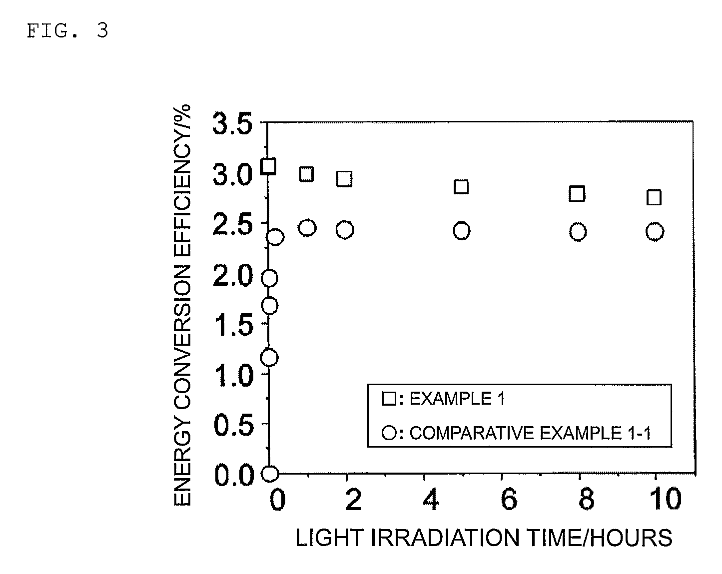
[0048]The hole-blocking layer of the present invention has excellent hole-blocking ability and light transmissivity. Therefore, a photoelectric conversion element comprising this hole-blocking layer has higher initial photoelectric conversion efficiency as compared with conventional photoelectric conversion elements. In a case where the photoelectric conversion element comprising the hole-blocking layer of the present invention is a solar cell, the solar cell exhibits excellent durability and is little prone to lose photoelectric conversion efficiency even under continued irradiation of light. Moreover, no special atmosphere control is necessary during the production of the hole-blocking layer, and no electrolysis equipment or cooling equipment is required. Also, the surface area per batch can be increased, and production made continuous, which translates into superior productivity.
[0049]Therefore, the present invention allows obtaining a photoelectric conversion element that has high photoelectric conversion efficiency and that exhibits high productivity and high quality stability. An organic solar cell panel or light-emitting device obtained by using such a photoelectric conversion element is likewise excellent in quality and economy.

Problems solved by technology

However, the development of organic thin-film solar cell-type photoelectric conversion elements has focused thus far only on enhancing photoelectric conversion efficiency, with no emphasis on technical developments from the viewpoint of productivity.

Method used


Image

  • Hole blocking layer and method for producing same, and photoelectric conversion element comprising the hole blocking layer and method for manufacturing same
  • Hole blocking layer and method for producing same, and photoelectric conversion element comprising the hole blocking layer and method for manufacturing same
  • Hole blocking layer and method for producing same, and photoelectric conversion element comprising the hole blocking layer and method for manufacturing same

Examples


first embodiment

I. First Embodiment

1. Hole-Blocking Layer

[0055]In the present invention, the hole-blocking layer denotes a layer that is disposed between an organic semiconductor layer and an electrode in an element that comprises the organic semiconductor layer and the electrode electrically connected to the organic semiconductor layer, and that suppresses electrical conduction between the organic semiconductor layer and the electrode from being carried by holes. The characteristic of suppressing the passage of holes, elicited by the hole-blocking layer, is referred to as hole-blocking ability.

[0056]The hole-blocking layer according to the present invention comprises substantially amorphous titanium oxide. Herein, “amorphous titanium oxide” denotes titanium oxide that contains also titanium oxide having an atomic ratio between oxygen and titanium other than the stoichiometric ratio (titanium:oxygen=1:2), and that has a structure lacking long-range order (over several hundred to several thousand at...

second embodiment

II. Second Embodiment

[0146]The present invention provides, as a second embodiment, a hole-blocking layer that is produced according to a process that has: a step of bringing into contact a nonaqueous solution (hereafter, “nonaqueous solution” for short) that contains an organic titanium compound represented by formula (2) below and a lower alkylamine (hereafter, “complexing agent”) such as diethylamine, triethylamine or the like, with the surface of a member (hereafter, “base material”) on which a hole-blocking layer is to be formed, to thereby form a liquid layer of the nonaqueous solution (hereafter, “nonaqueous solution layer”) on the surface of the base material; a step of forming, in the nonaqueous solution layer, a hydrolysis product of the organic titanium compound by hydrolyzing the organic titanium compound included in the nonaqueous solution layer; and a step of drying the nonaqueous solution layer that contains the hydrolysis product of the organic titanium compound.

Ti(OR...

example 1

[0176](1) Production of an Organic Thin-Film Solar Cell

[0177]An aqueous solution (hereafter, “aqueous solution” for short) was prepared that contained 0.03 mol / L of hydrogen peroxide (H2O2) and 0.03 mol / L of titanium (IV) oxysulfate (TiOSO4).

[0178]There was prepared a glass substrate with ITO film (Furuuchi Chemical) resulting from overlaying an ITO film, by sputtering, onto one of the surfaces of a glass substrate (22 mm×38 mm, thickness 1.1 mm). The thickness was 200 nm, and the sheet resistance of the ITO film that made up the light-transmitting electrode layer was 10 Ω / square.

[0179]The face of the glass substrate on the side opposite to the face on which the ITO film was formed was covered with a polyimide film, and the whole glass substrate was then boil-washed in 2-propanol.

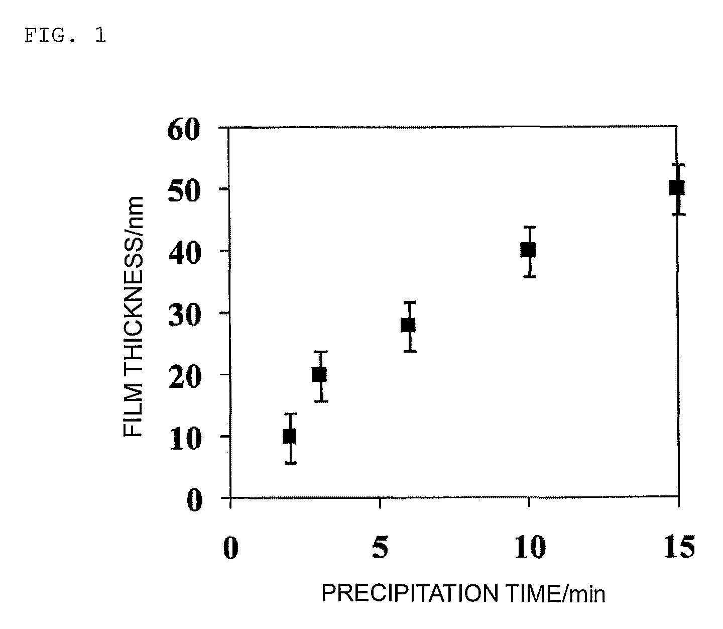
[0180]The glass substrate after washing, having the ITO film formed on one face thereof, and the other face covered by the polyimide film, was immersed for 5 minutes in the aqueous solution the temperature ...


PUM

PropertyMeasurementUnit
temperatureaaaaaaaaaa
thicknessaaaaaaaaaa
temperatureaaaaaaaaaa

Abstract

Provided is a hole-blocking layer which has excellent basic characteristics such as high photoelectric conversion efficiency, while exhibiting excellent productivity. The hole-blocking layer is produced by a process that has a step of bringing an aqueous solution containing hydrogen peroxide and titanium (IV) oxysulfate into contact with the surface of a member on which the hole-blocking layer is to be formed, and holding the contact between the aqueous solution and the member at 50 to 120° C., so that an amorphous titanium oxide precursor precipitates on the surface of the member; and a step of drying the amorphous titanium oxide precursor that has precipitated on the member.

Description

TECHNICAL FIELD[0001]The present invention relates to a hole-blocking layer that is disposed between an organic semiconductor layer and an electrode, and that suppresses electrical conduction between the organic semiconductor layer and the electrode from being carried by holes, and to a method for producing the hole-blocking layer, as well as to a photoelectric conversion element such as an organic thin-film solar cell and an organic EL element, that is provided with the hole-blocking layer.BACKGROUND ART[0002]Silicon-based solar cells, which are currently the dominant solar cell type, exhibit high photoelectric conversion efficiency, but incur significant environmental impact in terms of resources, carbon dioxide emissions during production, and cost. Therefore, research is being conducted, on a global scale, on solar cells that are clean, and have fewer resource constraints, in the form of photoelectric conversion elements that use organic semiconductor materials, in particular on...

Claims


Application Information

Patent Timeline
Patent Type & Authority Patents(United States)
IPC IPC(8): H01L51/54H01L51/42H01L51/44H01L51/48H01L51/56B82Y10/00H01L51/50H01L51/00
CPCH01L51/4253B82Y10/00H01L51/4273H01L51/5096H01L51/0036H01L51/0037H01L51/0047H01L2251/306Y02E10/549Y02P70/521Y02P70/50H10K85/1135H10K85/215H10K85/113H10K30/353H10K30/30H10K50/18H10K2102/102
Inventor KASAMA, YASUHIKOOMOTE, KENJISAIDA, MORIHIKOOIZUMI, HARUNASAGAMI, HIROYUKIYOKOO, KUNIYOSHISAITA, TAKASHITAKAHASHI, KOHSHINKUWABARA, TAKAYUKI
Owner IDEAL STAR
Learn More