

Plasma pre-clean module and process
a technology of pre-cleaning and plasma, applied in the direction of crystal growth process, polycrystalline material growth, chemically reactive gas, etc., can solve the problems of affecting the electrical performance of the desired material layer, increasing the number of defects, and interfering with the formation of a desired material layer over the substrate surfa
- Summary
- Abstract
- Description
- Claims
- Application Information
AI Technical Summary
Benefits of technology
Problems solved by technology
Method used
Image

Examples
Embodiment Construction
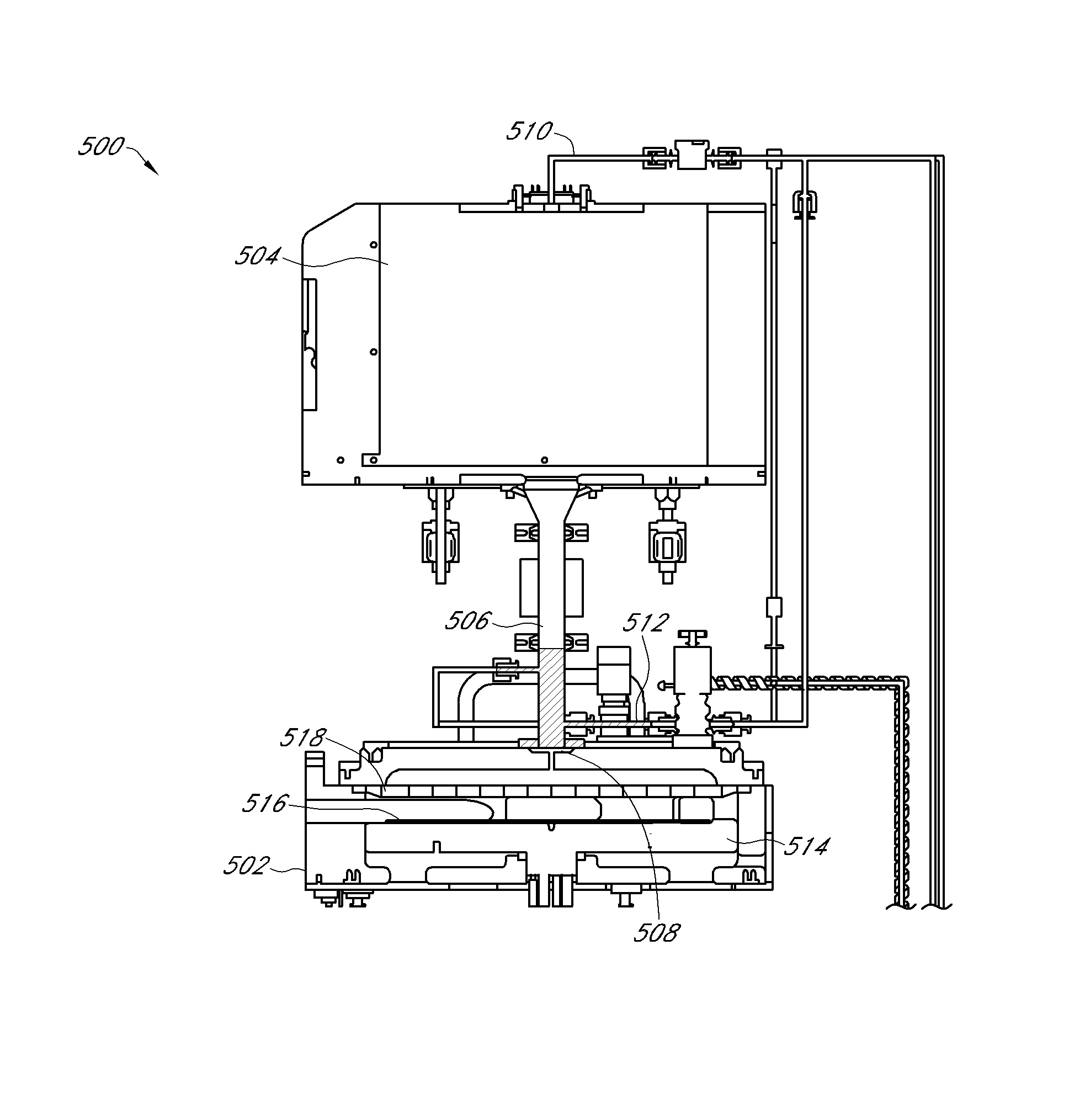
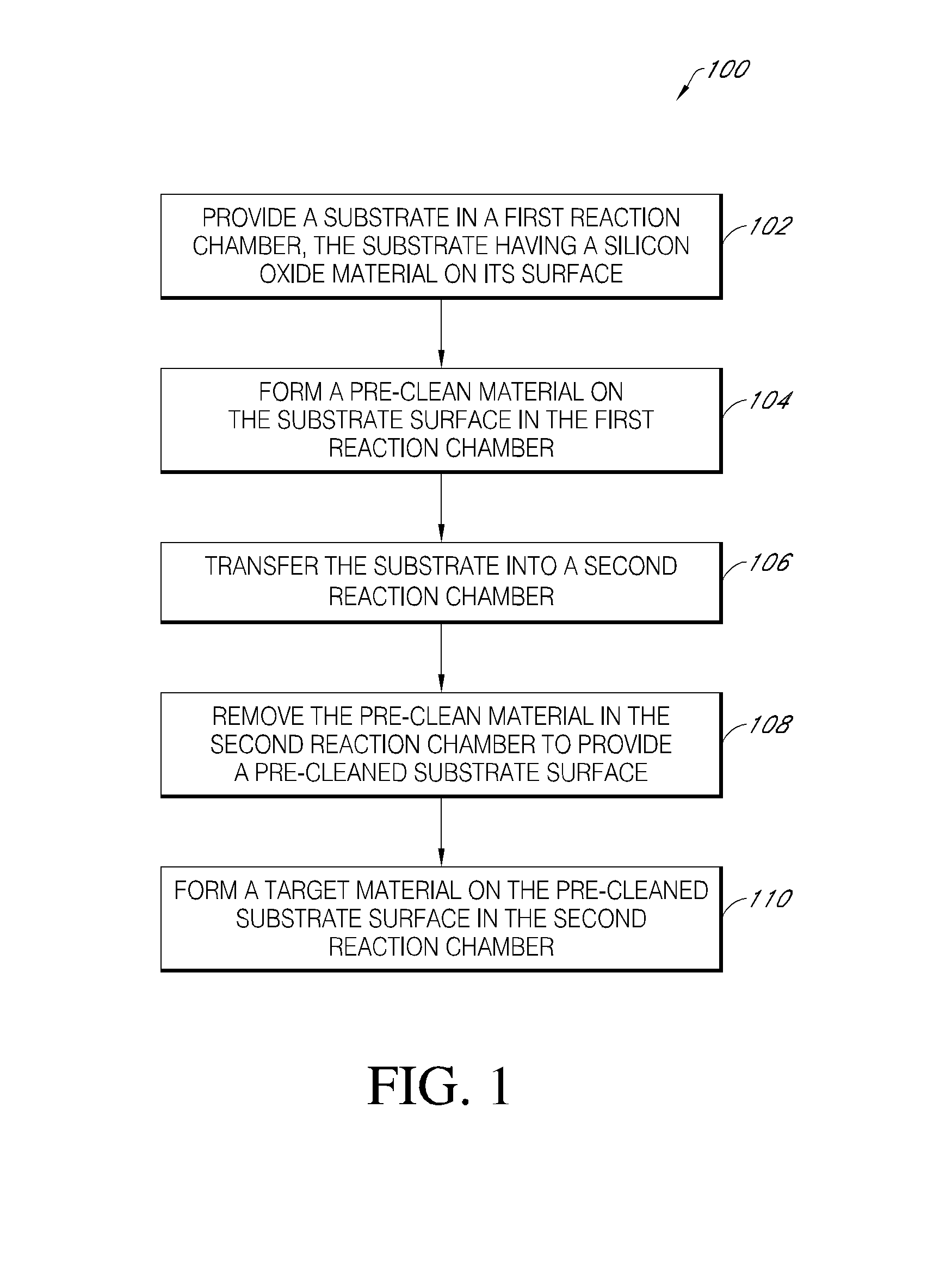
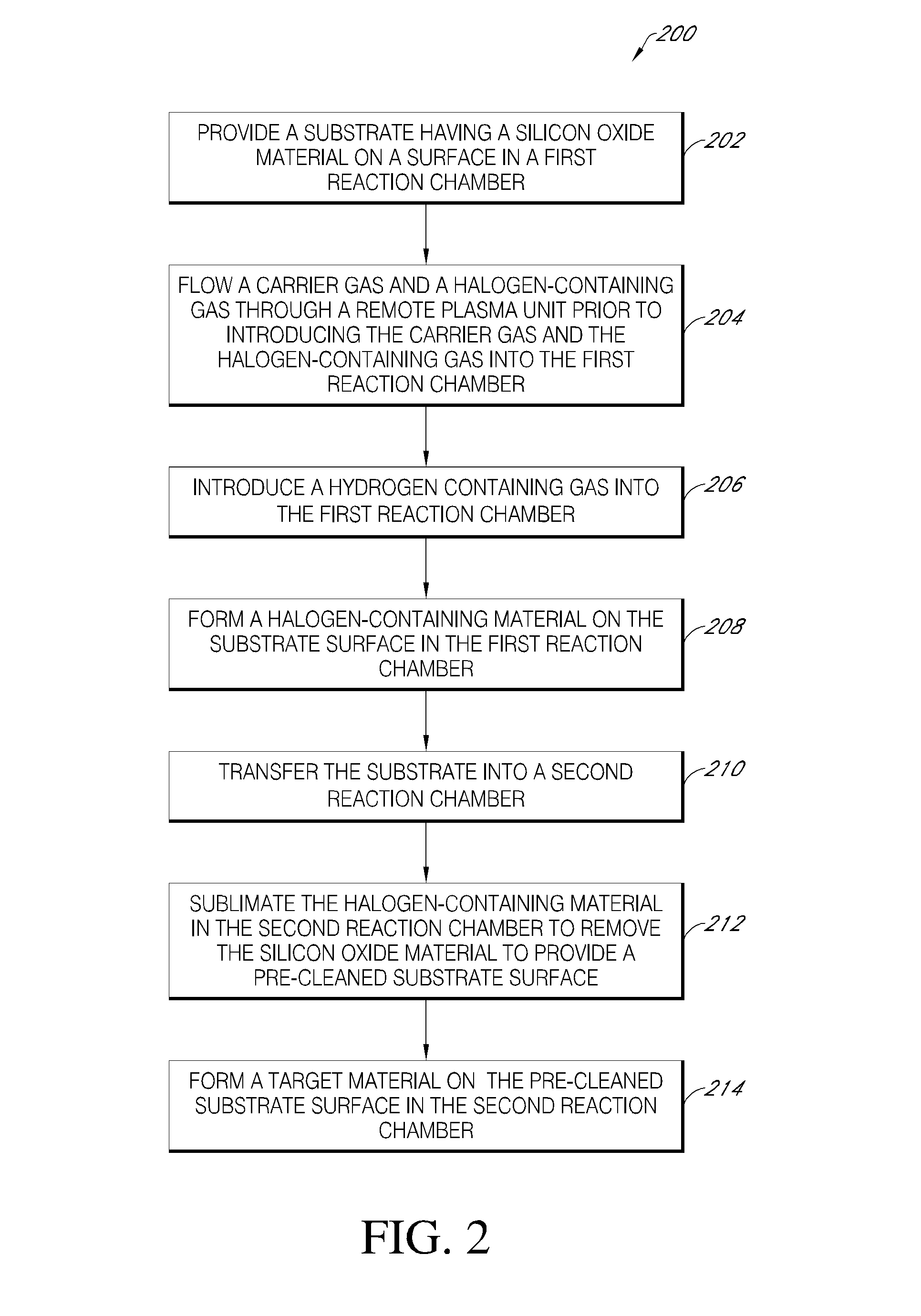
[0037]Various embodiments are described herein in relation to a pre-cleaning process for removing a silicon oxide material from an exposed surface of a substrate. It will be understood that the resulting pre-cleaned surface can provide a surface that facilitates the later formation of high quality layers of materials, such as the epitaxial growth of silicon.
[0038]In some embodiments, a process for integrated circuit fabrication can include pre-cleaning a substrate surface to remove an undesired material. The undesired material may comprise an oxide material (e.g., a native silicon oxide material formed on a silicon substrate) in some embodiments. Deposition of a pre-clean material and subsequent volatilization of the pre-clean material can advantageously cause removal of the oxide material from the substrate surface.
[0039]Without being limited by theory, it is believed that, to form the pre-clean material, reactant species flowed into the reaction chamber during the pre-clean proces...
PUM
| Property | Measurement | Unit |
|---|---|---|
| temperature | aaaaa | aaaaa |
| temperature | aaaaa | aaaaa |
| temperature | aaaaa | aaaaa |
Abstract
Description
Claims
Application Information