Tunnel field effect transistor and method for making thereof

a transistor and tunneling technology, applied in the direction of semiconductor devices, diodes, electrical apparatus, etc., can solve the problems of intrinsic channels between source and drain, difficulty in reducing supply voltage, and increasing power consumption, so called p-i-n

Active Publication Date: 2016-04-19
INTERUNIVERSITAIR MICRO ELECTRONICS CENT (IMEC VZW) +1
View PDF8 Cites 25 Cited by
  • Summary
  • Abstract
  • Description
  • Claims
  • Application Information

AI Technical Summary

Benefits of technology

[0019]According to embodiments, the vertical TFET may further comprise an auxiliary source layer comprising a semiconductor material different from the semiconducting core material, formed along the sidewalls of the vertical core region, the auxiliary source layer having a thickness of a few (e.g. 1 to 5 or 1 to 3) nanometers. This auxiliary source layer is for enhancing tunneling to the vertical drain region.
[0068]It is an advantage of different embodiments of the present invention that III-V based materials and process knowledge can be used to create nanowire TFET devices and that the nanowire TFET device manufacturing can be easily processed and integrated with current III-V-based technology devices.

Problems solved by technology

One of the problems due to the scaling down of CMOS transistors is that the power consumption keeps increasing.
This is partly because leakage currents are increasing (e.g. due to short channel effects) and because it becomes difficult to decrease the supply voltage.
A disadvantage of this approach is the presence of an intrinsic channel between source and drain, so called p-i-n TFET.
Since the tunnel direction is perpendicular to the gate dielectric, all parallel tunnel paths are switched on at the same time, leading to a sudden increase of current and sharp switching action.
However, since the tunnel junction is a surface parallel to the substrate, increasing the surface of the tunnel junction also increases the footprint of the TFET.

Method used


Image

  • Tunnel field effect transistor and method for making thereof
  • Tunnel field effect transistor and method for making thereof
  • Tunnel field effect transistor and method for making thereof

Examples


Embodiment Construction

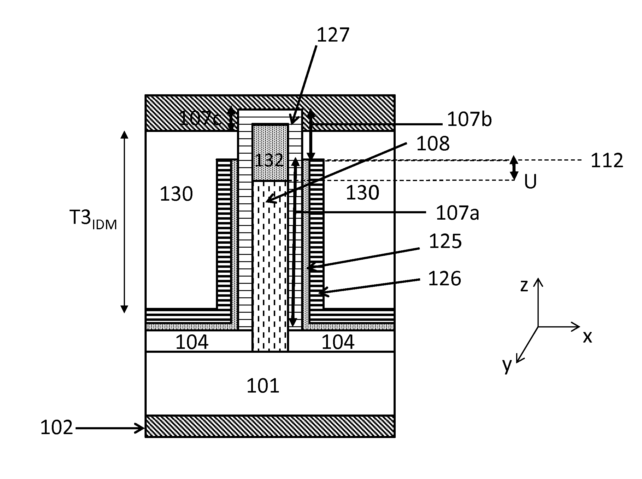
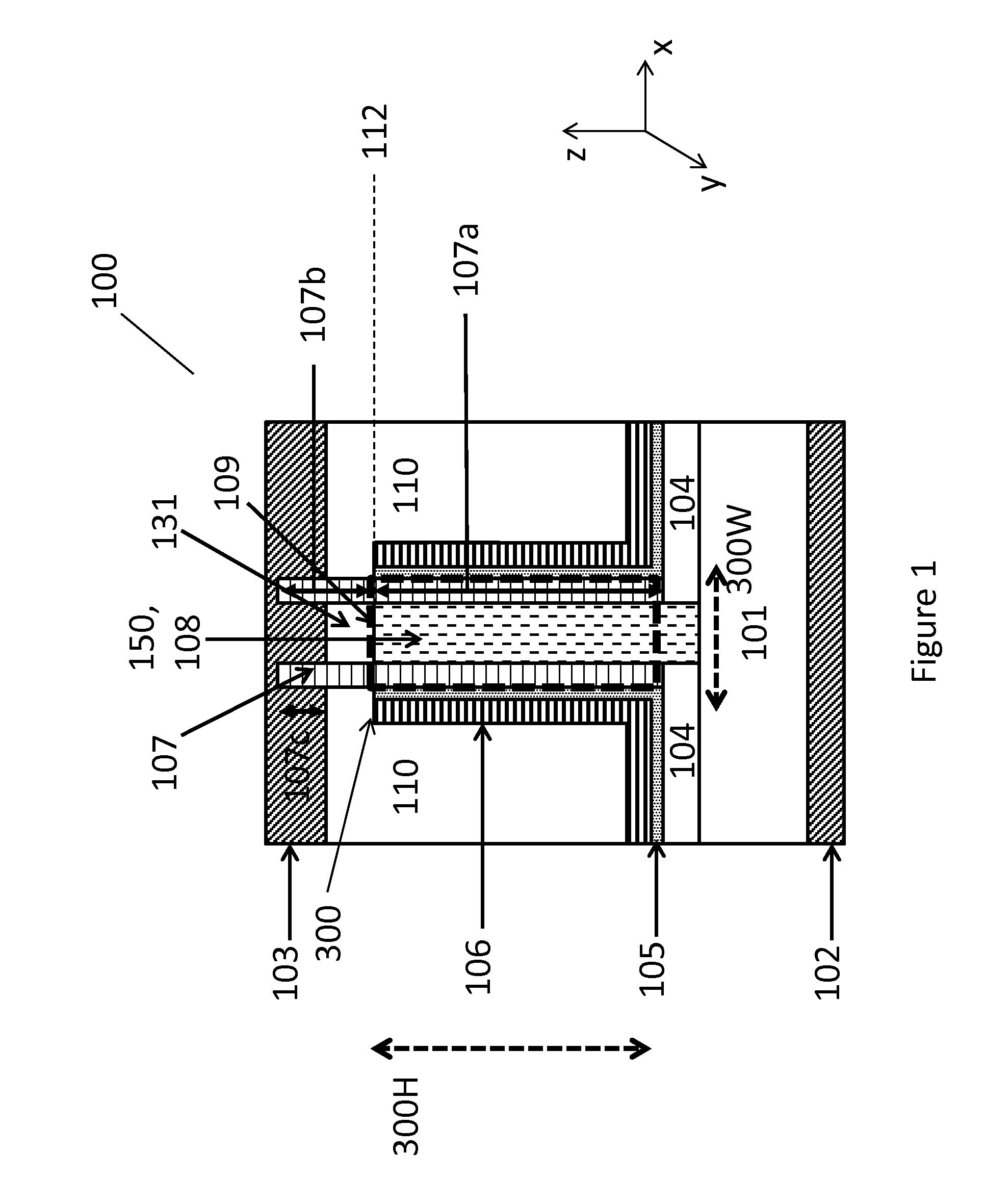
[0074]The disclosure will be further elucidated by means of the following description and the appended figures.

[0075]In the following detailed description, numerous specific details are set forth in order to provide a thorough understanding of the disclosure and how it may be practiced in particular embodiments. However, it will be understood that the present disclosure may be practiced without these specific details. In other instances, well-known methods, procedures and techniques have not been described in detail, so as not to obscure the present disclosure. While the present disclosure will be described with respect to particular embodiments and with reference to certain drawings, the disclosure is not limited hereto. The drawings included and described herein are schematic and are not limiting the scope of the disclosure. It is also noted that in the drawings, the size of some elements may be exaggerated and, therefore, not drawn to scale for illustrative purposes.

[0076]The pre...


PUM


Abstract

A vertical tunneling field effect transistor (TFET) and method for forming a vertical tunneling field effect transistor (TFET) is disclosed. The vertical tunneling field effect transistor TFET comprises a vertical core region, a vertical source region, a vertical drain region and a gate structure. The vertical core region is extending perpendicularly from a semiconductor substrate, having a top surface, consisting of a doped outer part and a middle part. The vertical source region of semiconducting core material comprises the doped outer part of the vertical core region. The vertical drain region of semiconducting drain material comprises along its longitudinal direction a first drain part and a second drain part, the first drain part either directly surrounding said vertical source region or directly sandwiching said vertical source region between two sub-parts of said first drain part, the second drain part located directly above and in contact with the first drain part. The gate structure comprises a gate dielectric layer directly aside of the first drain part of the vertical drain region and a gate layer directly aside of the gate dielectric layer. The second drain part is extending above the gate layer and gate dielectric layer. The vertical tunneling field effect transistor TFET further comprises a drain contact directly connected to a third drain part, the third drain part being an upper part of the second drain part of the vertical drain region. The vertical tunneling field effect transistor TFET further comprises a source contact electrically connected to the vertical source region. The vertical tunneling field effect transistor TFET further comprises a gate contact electrically connected to the gate layer.

Description

FIELD OF THE INVENTION[0001]The present disclosure relates to the field of semiconductor devices and nanotechnology.[0002]More specifically, the disclosure relates to a nanostructure semiconductor device, more specifically to a tunnel field effect transistor (TFET) wherein the injection mechanism is band-to-band tunneling.[0003]Furthermore the invention relates to a method for manufacturing a semiconductor device, more particularly to a method for fabricating tunnel field effect transistors. More specifically the fabrication method relates to but is not limited to non-planar / vertical technology, double gate technology, gate all-around technology and nanotechnology, wherein the latter includes implementations with integrated nanowires.STATE OF THE ART[0004]Nano electronic devices are generally fabricated on semiconductor substrates as integrated circuits. A complementary metal-oxide-semiconductor (CMOS) field effect transistor is one of the core elements of the integrated circuits. D...

Claims


Application Information

Patent Timeline
Patent Type & Authority Patents(United States)
IPC IPC(8): H01L29/76H01L29/78H01L29/66H01L29/739H01L29/06H01L29/205H01L29/51
CPCH01L29/068H01L29/0676H01L29/66356H01L29/66666H01L29/7391H01L29/7827H01L29/66977H01L29/205H01L29/517H01L29/7802
Inventor VERHULST, ANNE S.SMETS, QUENTIN
Owner INTERUNIVERSITAIR MICRO ELECTRONICS CENT (IMEC VZW)
Why Eureka
Try Eureka