Method for forming multi-element thin film constituted by at least five elements by PEALD

a multi-element, thin film technology, applied in the direction of coatings, chemical vapor deposition coatings, metallic material coating processes, etc., can solve the problems of difficult to deposit a dielectric film, difficult to deposit a high-quality multi-element dielectric film, and the need for good step coverage or conformality of the dielectric film

Active Publication Date: 2016-05-17
ASM IP HLDG BV
View PDF4 Cites 306 Cited by
  • Summary
  • Abstract
  • Description
  • Claims
  • Application Information

AI Technical Summary

Problems solved by technology

However, for a layer structure formed by damascene methods, such a dielectric film need not have a good step coverage or conformality.
It is difficult to deposit a dielectric film having the above properties by CVD.
Further, since a two-element film such as SiN may not have sufficient etch selectivity and good dielectric constant, a multi-element dielectric film consisting of more than two elements is under development.
However, it is not easy to deposit a high-quality multi-element dielectric film by ALD, since ALD using multiple elements involves problems such as interference with adsorption of one gas by adsorption of another gas.

Method used


Image

  • Method for forming multi-element thin film constituted by at least five elements by PEALD
  • Method for forming multi-element thin film constituted by at least five elements by PEALD
  • Method for forming multi-element thin film constituted by at least five elements by PEALD

Examples


examples

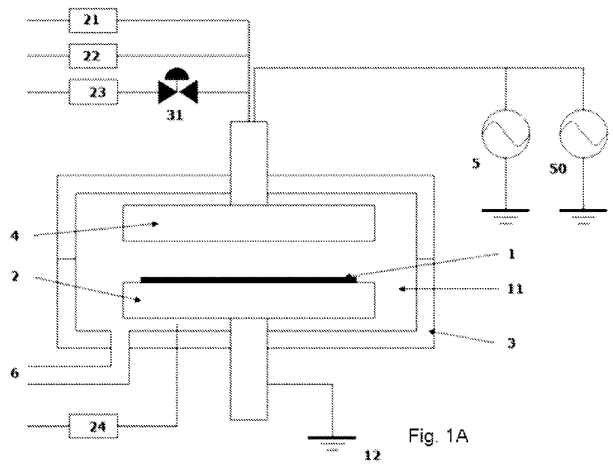
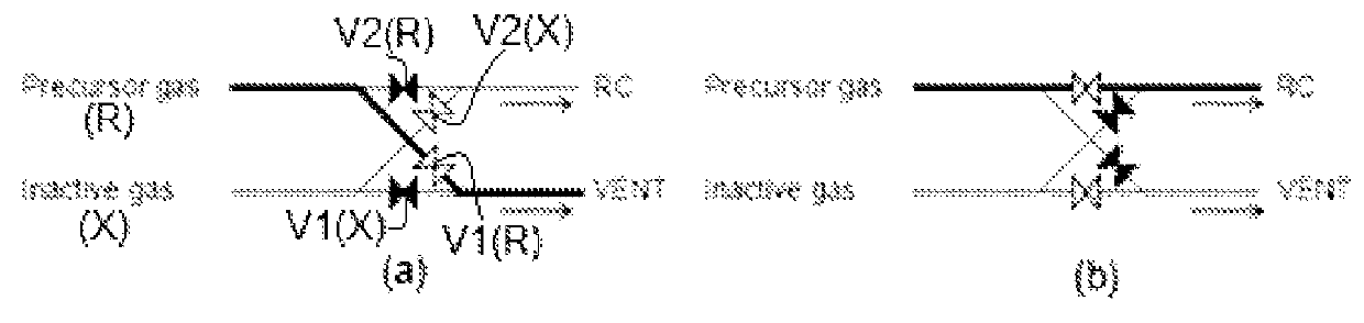
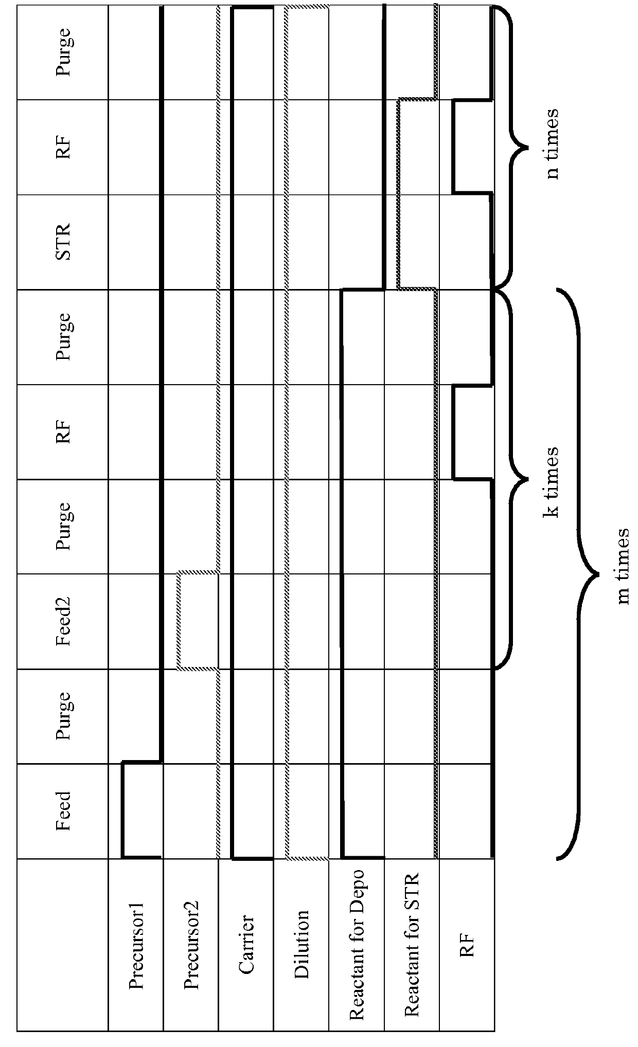
[0060]A multi-element dielectric film was formed on a Si substrate (0300 mm) having trenches with an aspect ratio of 3 (a width of 35 nm) by PEALD, one cycle of which was conducted under the common conditions shown in Table 3 (deposition cycle) and Table 4 (surface treatment cycle) below using the PEALD apparatus illustrated in FIG. 1A (including a modification illustrated in FIG. 1B) with the specific conditions and sequence indicated in Table 5 wherein “DCTDMS” represents dichlorotetradimehylsilane, “BT” represents boron triethyl, and “DIS” represents diiodosilane.

[0061]

TABLE 3(the numbers are approximate)Common Conditions for Deposition CycleSubstrate temperature400° C.Pressure400 PaCarrier gasArDilution gasArFlow rate of carrier gas (continuous)2000 sccmFlow rate of dilution gas (continuous)500 sccmRF power pulse1 secPurge0.5 sec

[0062]

TABLE 4(the numbers are approximate)Common Conditions for Surface Treatment CycleSubstrate temperatureSame as in deposition cyclePressureSame as i...


PUM

PropertyMeasurementUnit
thicknessaaaaaaaaaa
dielectric constantaaaaaaaaaa
temperatureaaaaaaaaaa

Abstract

A single-phase multi-element film constituted by at least four elements is formed on a substrate by plasma-enhanced atomic layer deposition (PEALD) conducting one or more process cycles. Each process cycle includes: (i) forming an integrated multi-element layer constituted by at least three elements on a substrate by PEALD using at least one precursor; and (ii) treating a surface of the integrated multi-element layer with a reactive oxygen, nitrogen, and/or carbon in the absence of a precursor for film formation so as to incorporate at least one new additional element selected from oxygen, nitrogen, and carbon into the integrated multi-element layer.

Description

BACKGROUND[0001]1. Field of the Invention[0002]The present invention relates generally to a method forming a single-phase multi-element film constituted by at least four elements on a substrate by plasma-enhanced atomic layer deposition (PEALD).[0003]2. Related Art[0004]Copper wiring has been used for logic devices, and dielectric films have been applied for copper wiring, which films are deposited by chemical vapor deposition (CVD) or spin-on dielectric (SOD). For example, a Cu-cap film used as a diffusion blocking film for copper is constituted by a dielectric material such as SiN. As miniaturization of devices progresses, a dielectric film having a dielectric coefficient (k value) as low as 5 or less is required. However, for a layer structure formed by damascene methods, such a dielectric film need not have a good step coverage or conformality. However, depending on the type of layer structure formed by, e.g., deposition and etching, a dielectric film is required to have a good ...

Claims


Application Information

Patent Timeline
Patent Type & Authority Patents(United States)
IPC IPC(8): H01L21/00H01L21/02
CPCH01L21/0228H01L21/02274H01L21/02323H01L21/02329H01L21/02321H01L21/02142H01L21/02126H01L21/0234H01L21/02112C23C16/45531C23C16/4554H01L21/02129
Inventor FUKAZAWA, ATSUKIFUKUDA, HIDEAKI
Owner ASM IP HLDG BV
Why Eureka
Try Eureka