Fused floating point datapath with correct rounding

a floating point datapath and correct rounding technology, applied in the field of performing floating point operations, can solve the problems of increasing the adder area of floating point, increasing the clock latency and the increase of the adder area, e.g., by 15%, and reducing the area consumed. , the effect of reducing the area consumed

US9348557B1Active Publication Date: 2016-05-24TAHOE RES LTD
3 Cites 20 Cited by

Patent Information

Authority / Receiving Office
US · United States
Current Assignee / Owner
Publication Date
2016-05-24

Smart Images

  • Figure 1
    Figure 1
  • Figure 2
    Figure 2
  • Figure 3
    Figure 3
Patent Text Reader

Abstract

In accordance with some embodiments, a floating point number datapath circuitry, e.g., within an integrated circuit programmable logic device is provided. The datapath circuitry may be used for computing a rounded absolute value of a mantissa of a floating point number. The floating point datapath circuitry may have only a single adder stage for computing a rounded absolute value of a mantissa of the floating point number based on one or more bits of an unrounded mantissa of the floating point number. The unrounded and rounded mantissas may include a sign bit, a sticky bit, a round bit, and / or a least significant bit, and / or other bits. The unrounded mantissa may be in a format that includes negative numbers (e.g., 2's complement) and the rounded mantissa may be in a format that may include a portion of the floating point number represented as a positive number, (e.g., signed magnitude).
Need to check novelty before this filing date? Find Prior Art

Description

FIELD OF THE INVENTION

[0001] This invention relates to a performing floating point operations in programmable integrated circuit devices, including the use of specialized processing blocks, which may be included in such devices, to perform floating point operations.BACKGROUND

[0002] Considering a programmable logic device (PLD) as one example of an integrated circuit device, as applications for which PLDs are used increase in complexity, it has become more common to design PLDs to include configurable specialized processing blocks in addition to blocks of generic programmable logic resources. Such configurable specialized processing blocks may include a concentration of circuitry on a PLD that has been partly or fully hardwired to perform one or more specific tasks, such as a logical or a mathematical operation. A configurable specialized processing block may also contain one or more specialized structures, such as an array of configurable memory elements. Examples of structures that a...

Examples

Embodiment Construction

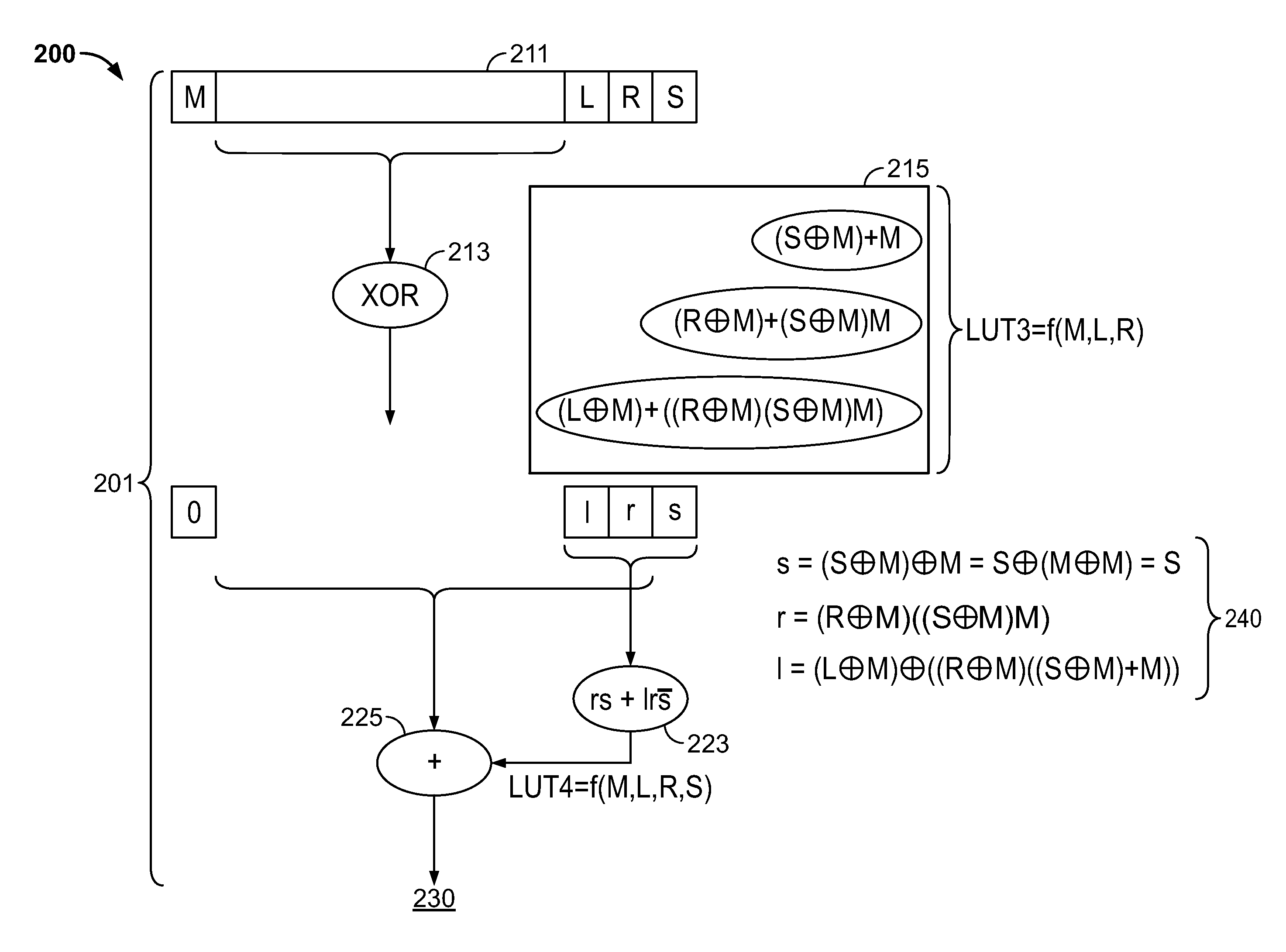
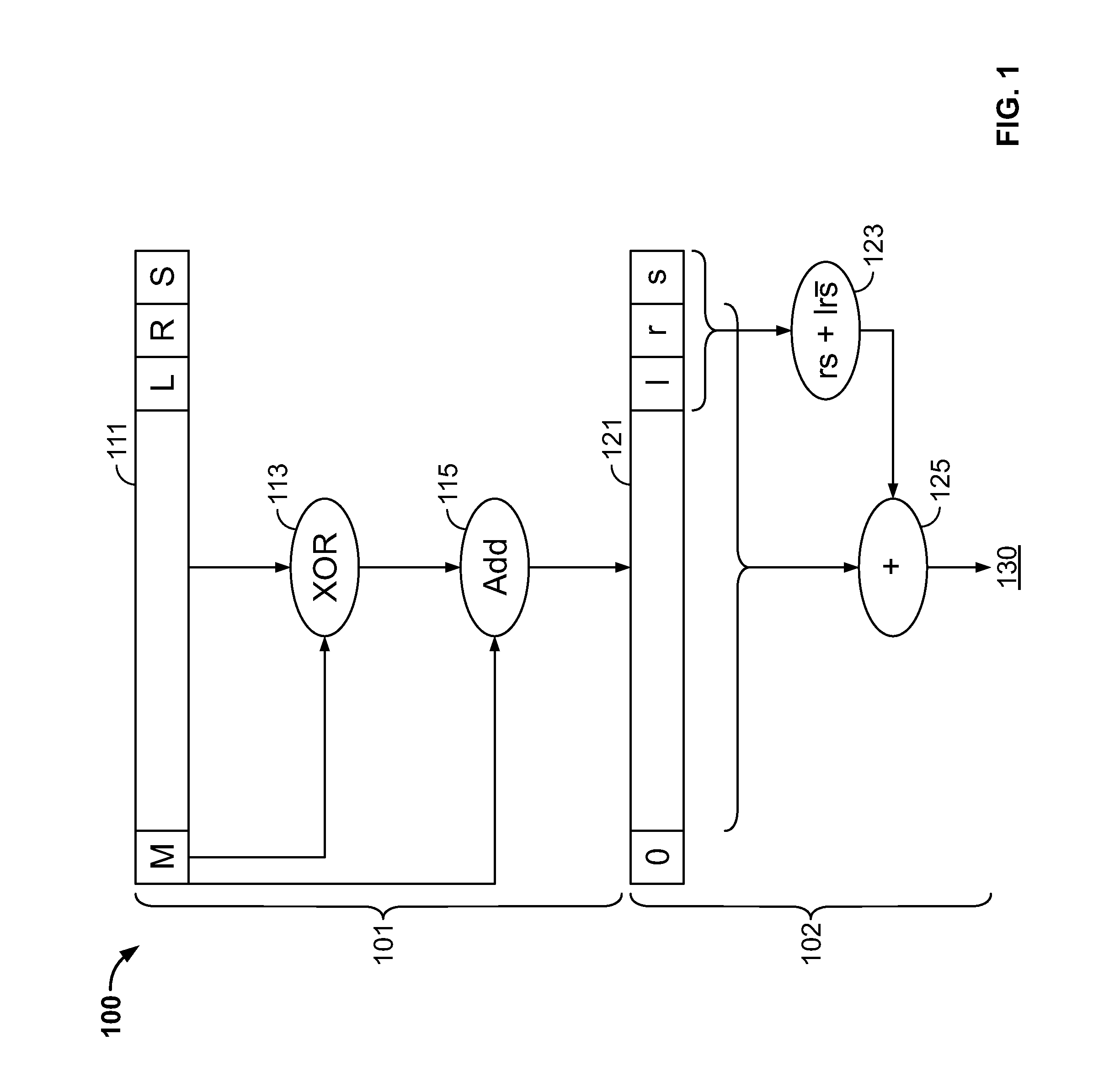
[0016]FIG. 1 shows a logical representation of exemplary datapath circuitry 100 in which the ABS and rounding functions are performed on a floating point number in a datapath using a two adder structure according to an embodiment of the present invention. In this logical representation, details of implementation, such as registers and some programmable routing features—such as multiplexers that may allow the output of a particular element to be routed directly out of circuitry 100—are omitted to simplify discussion. In addition, some elements that are shown may, in an actual embodiment, be implemented more than once. For example, XOR logic 113 may actually represent two or more XOR gates.

[0017]In the logical representation of FIG. 1, datapath circuitry 100 may be implemented using FPC technology and located within any configurable specialized processing block. The floating-point ABS function circuitry 101 and rounding function circuitry 102, that are included as a part of circuitry ...