Plasmon field effect transistor

Active Publication Date: 2016-06-14
KIM SUNG JIN
View PDF3 Cites 32 Cited by
  • Summary
  • Abstract
  • Description
  • Claims
  • Application Information

AI Technical Summary

Benefits of technology

[0012]A field effect transistor (FET) is provided. The FET includes a first material layer. The first material layer includes one of Si layer, semiconducting metal oxide layer, group III-V compound semiconductor layer, Group II-VI compound semiconductor layer and group III-nitride semiconductor layer. The FET includes a second material layer such as an insulating dielectric layer. The second material layer includes one of a Silicon Dioxide (SiO2) layer Aluminum Oxide (Al2O3) layer and Silicon Nitride (SiNx) layer. The FET includes a third material layer. The third material layer includes a n-type silicon substrate layer and an insulating layer with conducting metal acting as a g

Problems solved by technology

Semiconductor 8 and other similar existing technologies exhibit very low responsivity (A/W) or external quantum efficiency due to limited absorption in the thin metal structure and inefficient hot electron diffusion from metal to semiconductor.
Another issue with semiconductor 8 and these existing technologies is that the Schottky

Method used


Image

  • Plasmon field effect transistor
  • Plasmon field effect transistor
  • Plasmon field effect transistor

Examples


Embodiment Construction

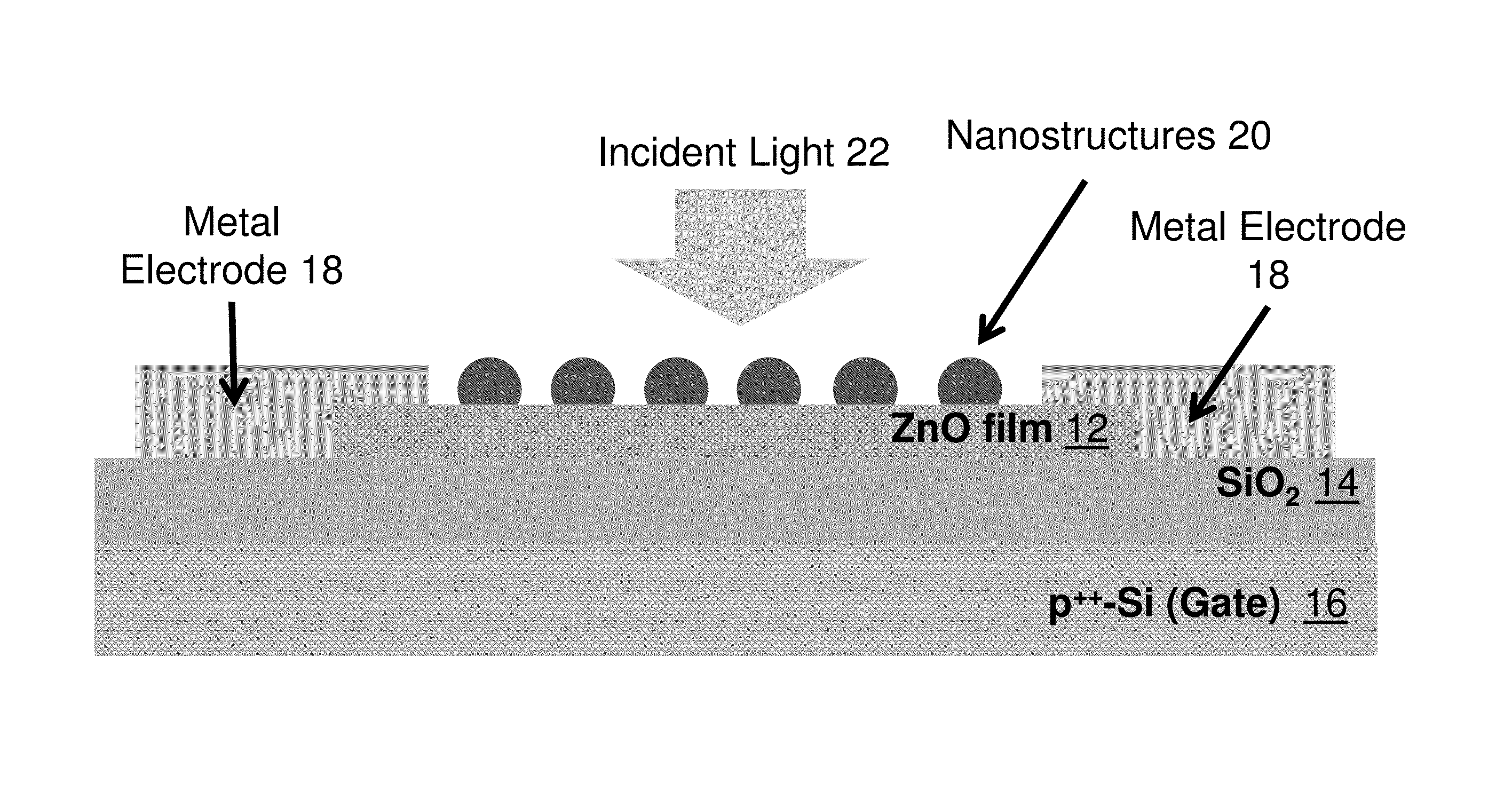
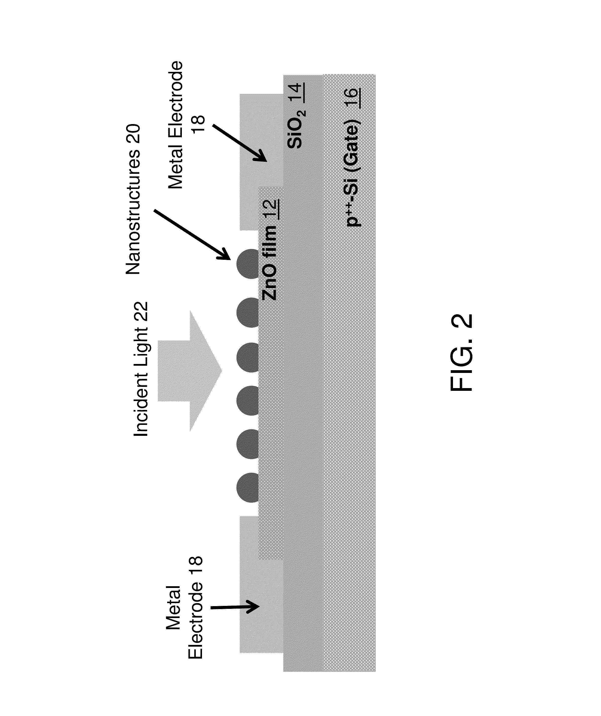
[0039]The present invention advantageously provides a method, device and system for detecting electromagnetic energy, and in particular for detecting electromagnetic energy with a plasmon Field Effect Transistor. Accordingly, the system and method components have been represented where appropriate by conventional symbols in the drawings, showing only those specific details that are pertinent to understanding the embodiments of the present invention so as not to obscure the disclosure with details that will be readily apparent to those of ordinary skill in the art having the benefit of the description herein.

[0040]Referring now to the drawing figures in which like reference designators refer to like elements there is shown in FIG. 2 an exemplary plasmon Field Effect Transistor (FET) in accordance with the principles of the present invention and designated generally as “10.” FET 10 may be based on any semiconducting materials and may include organic and inorganic, N and P types. FET 1...


PUM


Abstract

A field effect transistor (FET) is provided. The FET includes a first material layer, second material layer and a third material layer. The third material layer includes an n-type silicon substrate layer and a gate electrode. The gate electrode includes an insulating substrate with at least one conducting metal. The second material layer is disposed on the third material layer. The first material layer is disposed on the second material layer. A source electrode is disposed on the first material layer. A drain electrode is disposed on the first material layer. A plurality of gold nanostructures are disposed on an active channel of the FET. The plurality of gold nanostructures are electrically isolated from the source electrode, drain electrode and gate electrode. The plurality of gold nanostructures contribute to a drain current of the FET based at least in part on plasmonic absorption of photons.

Description

CROSS-REFERENCE TO RELATED APPLICATION[0001]This application is related to and claims priority to U.S. Provisional Patent Application No. 61 / 759,595, filed Feb. 1, 2013, entitled PLASMON FIELD EFFECT TRANSISTOR, the entirety of which is incorporated herein by reference.FIELD OF THE INVENTION[0002]The present invention relates to a method, device and system for detecting electromagnetic energy, and in particular for detecting electromagnetic energy with a plasmon Field Effect Transistor.BACKGROUND OF THE INVENTION[0003]The interests on plasmons, associated with nanostructured metals, have remarkably increased in the past decade. Surface plasmon resonance (SPR) sensor is one of the successful applications, which is widely used in biomedical research. On the other hand, localized surface plasmon resonance (LSPR) is also widely studied in a broad range of applications. The distinct property of LSPR is a tailored and sharp absorption and scattering peaks depending on the shape and sizes ...

Claims


Application Information

Patent Timeline
IPC IPC(8): H01L31/062H01L31/113H01L31/0352
CPCH01L31/1136H01L31/035272G01N21/554G01N27/4146H01L31/02327
Inventor KIM, SUNG JINYUN, JUHYUNG
Owner KIM SUNG JIN
Why Eureka
Try Eureka