Highly reliable nonvolatile memory and manufacturing method thereof

a nonvolatile memory, high-resistance technology, applied in the direction of digital storage, instruments, semiconductor devices, etc., can solve the problems of increasing the severity of reliability problems, the uniformity of memory, and the scaling of dram, sram and flash is reaching the limit, so as to increase the effect of increasing the uniformity of resistive random access memory

Inactive Publication Date: 2016-06-28
PEKING UNIV
View PDF21 Cites 4 Cited by
  • Summary
  • Abstract
  • Description
  • Claims
  • Application Information

AI Technical Summary

Benefits of technology

[0006]Directed to the above-mentioned problems, an object of the present invention is to increase the uniformity of the resistive random access memory and solve the reliability problem existed in the resistive random access memory. According to the present invention, the uniformity and reliability of the resistive random access memory can be effectively increased by adopting a method in which a doping technology and a double-layer resistive material forming technology are combined.
[0028]The resistive random access memory provided by the present invention has the following advantages.
[0029](1) The fabrication process is compatible with a CMOS process and thus is easily to be implemented.
[0030](2) The uniformity of the resistive random access memory can be effectively increased by the doping process. Both of the above-mentioned two conditions for the doped metal M2 can increase the concentration of oxygen vacancies surrounding M2 so that the conductive channel formed by the oxygen vacancies is formed along the doping path, and thus the poor uniformity problem caused by the random conductive filaments can be avoided. Specifically, as to the first condition that Gibbs free energy ΔM1 of the metal M1 reacting with oxygen to form an oxide is lower than Gibbs free energy ΔM2 of the metal M2 reacting with oxygen to form an oxide, that is, the metal M1 corresponding to the resistive material layer is more easily to be reacted with oxygen. In other words, the surrounding of M2 is of a higher concentration of oxygen vacancies. On the other hand, owing to the second condition that a valence state of the metal M2 in its corresponding oxide is lower than a valence state of the metal M1 in its corresponding oxide, the forming energy of the oxygen vacancies surrounding M2 is reduced, that is, the concentration of the oxygen vacancies surrounding M2 is higher.
[0031](3) By introducing the thin metal oxygen storage layer between the resistive material layer and top electrodes, the reliability problems existed in the resistive random access memory is solved. Since Gibbs free energy ΔM1 of the metal M1 reacting with oxygen to form an oxide is higher than Gibbs free energy ΔM3 of the metal M3 reacting with oxygen to form an oxide, that is, the metal M3 is more easily to be reacted with oxygen, the directionally-moved oxygen ions are reacted with the metal M3 during the forming / setting process at an interface between the resistive material layer and the metal oxygen storage layer and is stored in a manner of oxide. Thus, the oxygen ions can be prevented from diffusing into the environment along the metal of the top electrodes and affecting the durability of the resistive random access memory.

Problems solved by technology

However, as the technology advances, that is, as the critical dimension continuously reduces and the integration degree constantly increases, the scaling of the DRAM, SRAM and Flash is reaching the limitation, especially in the circumstance of entering a nanometer technology node.
In particular, the performance of the parameters of the nonvolatile memory fluctuates randomly and significantly, resulting in more and more severed reliability problems.
Because of the fact that the formation location, the length and the size of the conductive channel in the resistive random access memory are random, parameters exhibited by the resistive random access memories may fluctuate depending on various memories or various switching processes, and thus a uniformity problem of the memories is caused.
During the repeated reading operations, the metal ions and the oxygen vacancies may diffuse into surroundings so that the performance of the resistive random access memory is deteriorated, which causes a reliability problem.

Method used


Image

  • Highly reliable nonvolatile memory and manufacturing method thereof
  • Highly reliable nonvolatile memory and manufacturing method thereof
  • Highly reliable nonvolatile memory and manufacturing method thereof

Examples


Embodiment Construction

[0042]Hereinafter, technical solutions of embodiments of the present invention will be clearly and fully described in conjunction with the accompanying drawings. However, it is understood that the described embodiments are only part of the implementations of the present invention, rather than all of them. Based on the embodiments of the present invention, other implementations made by those skilled in the art without paying creative efforts will fall into the protection scope of the present invention.

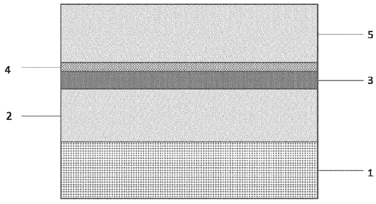
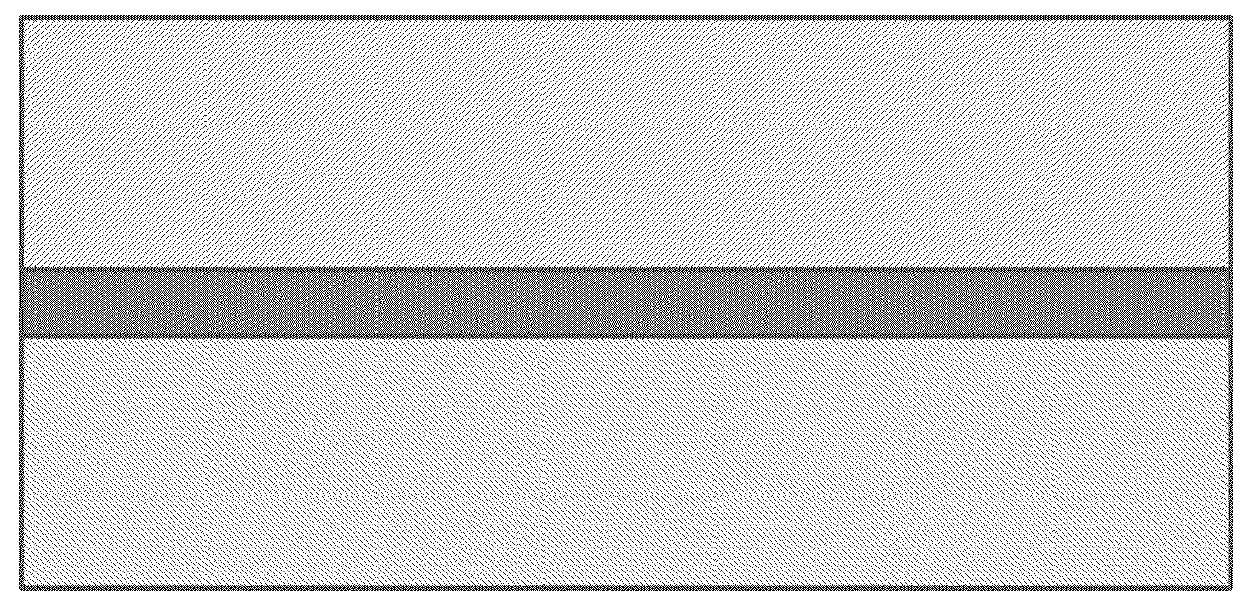
[0043]FIG. 2 shows a structure of a highly reliable nonvolatile memory, which includes, from the bottom up a substrate 1, a bottom electrode 2, a resistive material layer 3 doped with metal, a thin metal oxygen storage layer 4 and a top electrode 5.

[0044]The shown structure is described in details as follows.

[0045](1) The substrate 1 is formed of Si or other supporting substrates.

[0046](2) The bottom electrode 2 and the top electrode 5 (defined as M01 and M02, respectively) are formed o...


PUM

PropertyMeasurementUnit
thicknessaaaaaaaaaa
thicknessaaaaaaaaaa
thicknessaaaaaaaaaa

Abstract

The present invention relates to a highly reliable nonvolatile memory and a manufacturing method thereof. The nonvolatile memory comprises top electrodes, bottom electrodes and a resistive material layer disposed therebetween, wherein the top electrodes are positioned on top in the memory; the bottom electrodes are positioned on a substrate; metal oxide for forming the resistive material layer is doped with metal; and a metal oxygen storage layer is further disposed between the top electrodes and the resistive material layer. The manufacturing method adopts a method in which a doping method and a double-layer forming method are combined, so that the highly reliable and highly uniform resistive random access memory can be fabricated and accordingly the performance of the memory can be increased.

Description

FIELD OF THE INVENTION[0001]The present invention relates to a resistive random access memory (RRAM), and in particular, relates to a highly reliable and highly uniform memory and a manufacturing method thereof, which is in a field of manufacturing a nonvolatile memory and optimizing the performance of the nonvolatile memory in a CMOS ultra-large-scale integrated circuit (ULSI).BACKGROUND OF THE INVENTION[0002]The semiconductors memory has been playing core role in the development of the semiconductor technology, holding an irreplaceable position in various information technology (IT) fields. Currently, the mainstream semiconductor memory includes a volatile dynamic random access memory (DRAM) and static random access memory (SRAM), and a nonvolatile flash memory (Flash). However, as the technology advances, that is, as the critical dimension continuously reduces and the integration degree constantly increases, the scaling of the DRAM, SRAM and Flash is reaching the limitation, espe...

Claims


Application Information

Patent Timeline
Patent Type & Authority Patents(United States)
IPC IPC(8): H01L27/115H01L45/00G11C13/00H01L27/11
CPCH01L45/1625H01L45/1666H01L45/146G11C13/0007H01L45/08H01L45/085H01L45/122H01L45/1233H01L45/1253H01L45/1266H01L45/1273G11C2213/56H01L27/1112H10N70/245H10N70/24H10N70/8416H10N70/8418H10N70/026H10N70/8833H10N70/826H10B10/15H10N70/061H10N70/821H10N70/841
Inventor HUANG, RUYU, MUXICAI, YIMAOBAI, WENLIANGHUANG, YINGLONG
Owner PEKING UNIV
Why Eureka
Try Eureka