Semiconductor device and manufacturing method of conductive structure in semiconductor device

a semiconductor device and semiconductor technology, applied in semiconductor devices, semiconductor/solid-state device details, electrical apparatus, etc., can solve the problems of yield loss, more complicated circuit design of new generation products, and smaller circuit designs of products of the new generation, so as to enhance the process window and the manufacturing yield

Active Publication Date: 2016-07-19
MARLIN SEMICON LTD
View PDF9 Cites 15 Cited by
  • Summary
  • Abstract
  • Description
  • Claims
  • Application Information

AI Technical Summary

Benefits of technology

[0007]According to the manufacturing method of the conductive structure in the semiconductor device, the conductive structure between the gate structures may be formed and self-aligned because the air void is formed in the space between the gate structures before the opening penetrating the second dielectric layer is formed. The manufacturing yield and the process window may be enhanced accordingly.

Problems solved by technology

The development of semiconductor integrated circuit technology progresses continuously and circuit designs in products of the new generation become smaller and more complicated than those of the former generation.
However, it is difficult to form conductive plugs in the extremely small space between the gate lines because of the exposure limitation of the photolithography process, and mis-alignments occurred in the photolithography process for forming the conductive plugs between the gate lines may result in yield loss because the process window is too limited.

Method used


Image

  • Semiconductor device and manufacturing method of conductive structure in semiconductor device
  • Semiconductor device and manufacturing method of conductive structure in semiconductor device
  • Semiconductor device and manufacturing method of conductive structure in semiconductor device

Examples


Embodiment Construction

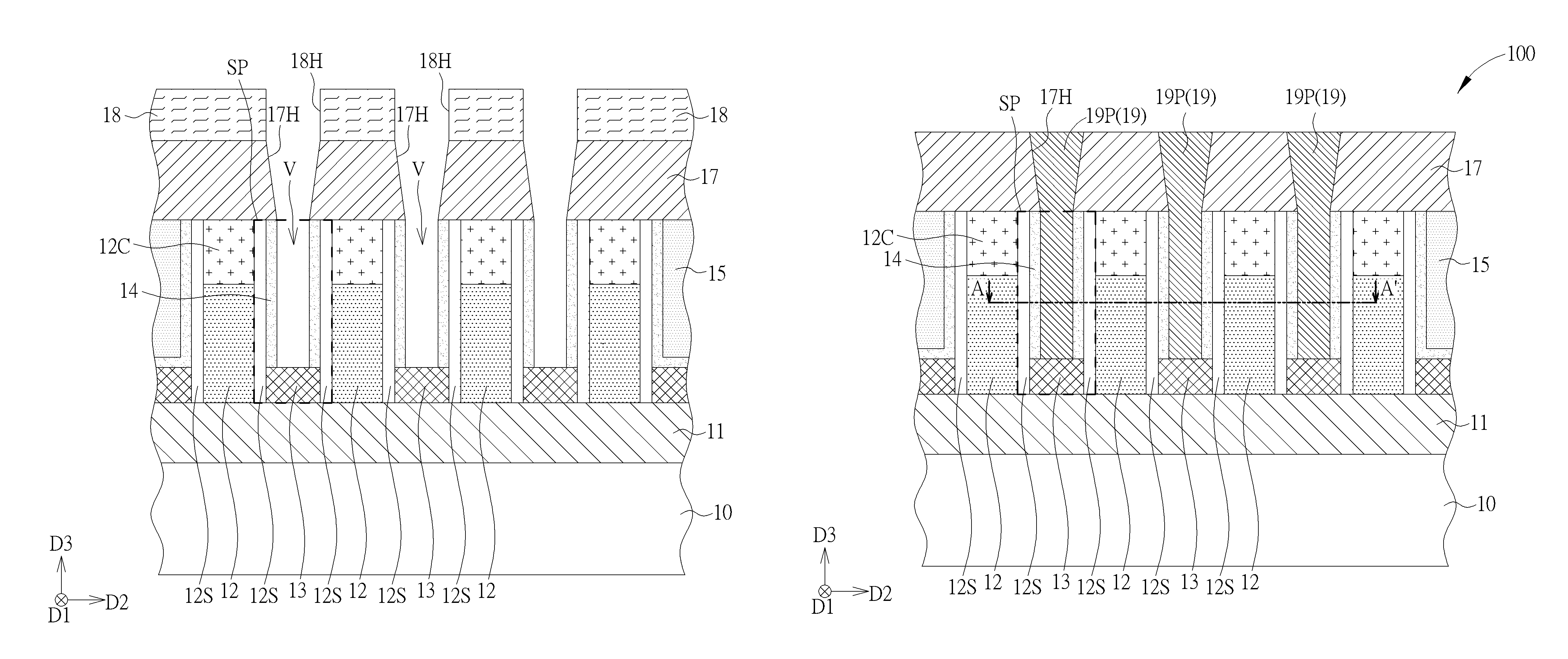
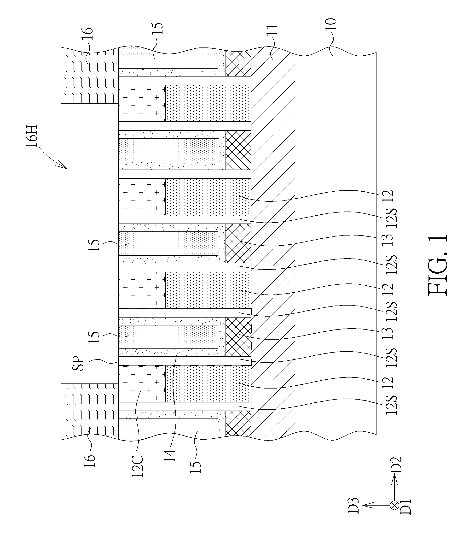
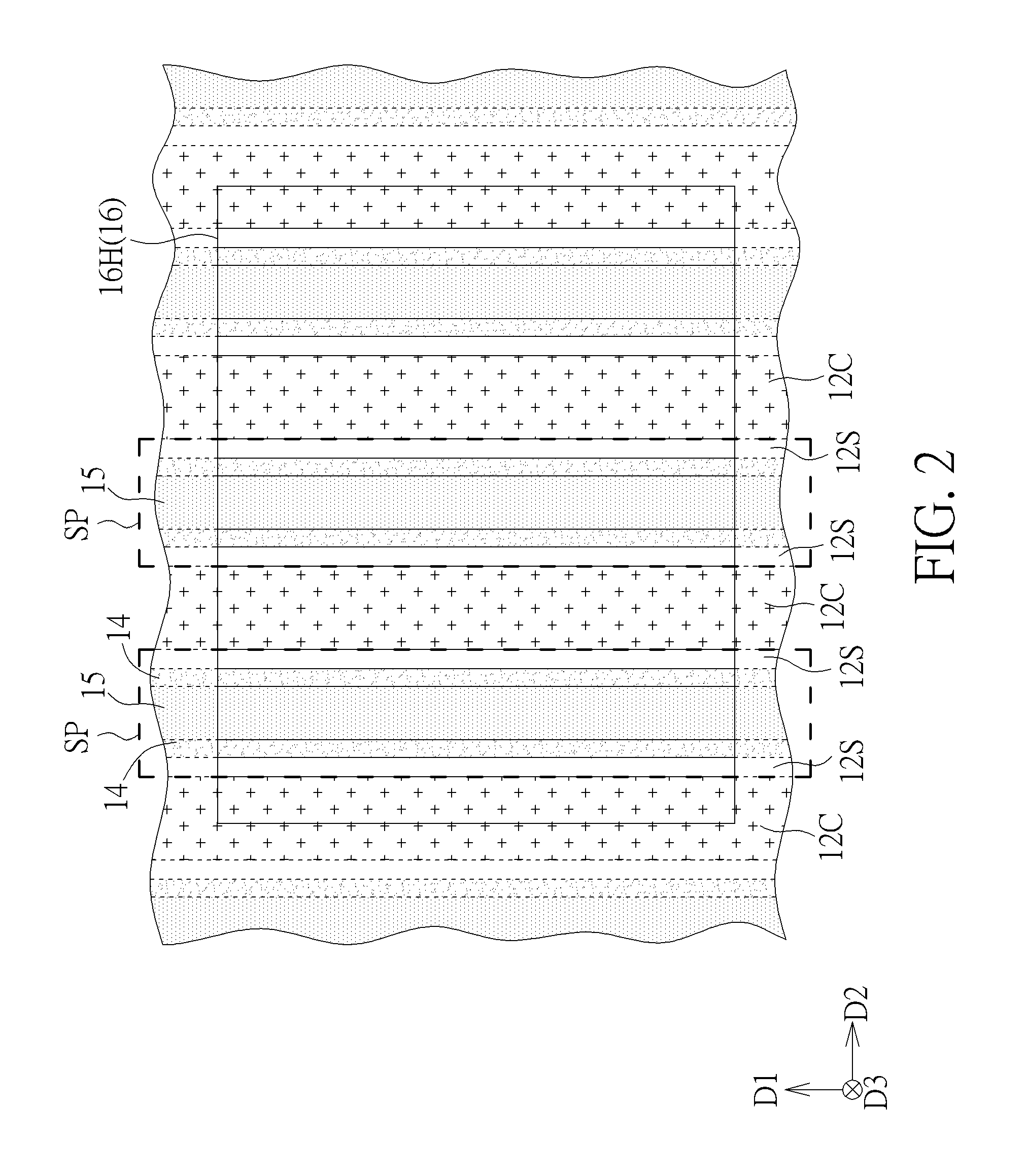
[0023]Please refer to FIGS. 1-9. FIGS. 1-9 are schematic drawings illustrating a manufacturing method of a conductive structure in a semiconductor device according to a first embodiment of the present invention. The manufacturing method of the conductive structure in this embodiment includes the following steps. As shown in FIG. 1 and FIG. 2, a semiconductor structure 11 is formed on a substrate 10. The substrate 10 may include a silicon substrate, an epitaxial silicon substrate, a silicon germanium substrate, a silicon carbide substrate, or a silicon-on-insulator (SOI) substrate, but not limited thereto. The semiconductor structure 11 may be a semiconductor layer, a semiconductor fin structure, or other appropriate semiconductor structures. A plurality of gate structures 12 are formed on the semiconductor structure 11. In this embodiment, the gate structures 12 may include gate lines extending in a first direction D1, but not limited thereto. The gate structures 12 are disposed par...


PUM


Abstract

A manufacturing method of a conductive structure in a semiconductor device includes the following steps. A plurality of gate structures are formed on a semiconductor structure, and a first dielectric layer is formed in space between the gate structures. A first process is then performed to remove at least a part of the first dielectric layer in the space between the gate structures. A second dielectric layer is then formed and covers the gate structures so as to form at least one air void in the space between the gate structures. A second process is performed to form at least one opening penetrating the second dielectric layer and exposing the air void. The air void exposed by the opening is then filled with at least one conductive material for forming a conductive structure between the gate structures.

Description

BACKGROUND OF THE INVENTION[0001]1. Field of the Invention[0002]The present invention relates to a semiconductor device and a manufacturing method of a conductive structure in a semiconductor device, and more particularly, to a semiconductor device including a self-aligned conductive structure and a manufacturing method of the self-aligned conductive structure in the semiconductor device.[0003]2. Description of the Prior Art[0004]The development of semiconductor integrated circuit technology progresses continuously and circuit designs in products of the new generation become smaller and more complicated than those of the former generation. The amount and the density of the functional devices in each chip region are increased constantly according to the requirements of innovated products, and the size of each device has to become smaller accordingly. For example, in field effect transistors, the spacing between gate lines becomes smaller for enhancing the integrity of the integrated ...

Claims


Application Information

Patent Timeline
Patent Type & Authority Patents(United States)
IPC IPC(8): H01L21/8234H01L29/66H01L21/311H01L21/3213H01L27/088H01L21/027H01L29/06
CPCH01L21/823437H01L21/823475H01L21/823418H01L21/32139H01L21/31144H01L29/66545H01L27/088H01L29/0653H01L29/665H01L21/31111H01L21/0274H01L21/823425H01L23/485H01L21/76801H01L21/76831H01L29/78H01L29/41791H01L21/76897H01L29/41783H01L29/66795H01L29/785
Inventor TUNG, YU-CHENGLIOU, EN-CHIUAN
Owner MARLIN SEMICON LTD
Why Eureka
Try Eureka