High data rate long reach transceiver using wavelength multiplexed architecture

Active Publication Date: 2016-08-23
NEOPHOTONICS CORP
View PDF28 Cites 1 Cited by
  • Summary
  • Abstract
  • Description
  • Claims
  • Application Information

AI Technical Summary

Benefits of technology

The invention describes an architecture that uses an array of directly modulated lasers on a compound semiconductor substrate. The lasers have wide wavelength spacing, which allows for uncooled or semi-cooled operation. This results in a simple and low-cost chip that generates multiple modulated signals simultaneously. The architecture also includes a wavelength-selective combiner and a demultiplexer to track the transmitter. The lasers have high efficiency and low thresholds, which enables the use of silicon drivers even at high speeds. The extinction ratio is kept low for good chirp characteristics. The wavelength-selective combiner can be an arrayed waveguide grating, which is compact and has a high resolution. The output of the combiner can be coupled to a single mode fiber with or without an optical isolator in between.

Problems solved by technology

The lower drive speed of the lasers allows the use of low cost silicon driver chips, yet the array can have an aggregate bandwidth that is enormous.
In contrast a single directly modulated laser is almost impossible at 40 Gb / s, and if it were so, the reach would be less than 1 Km and would require very expensive compound semiconductor drive electronics.

Method used


Image

  • High data rate long reach transceiver using wavelength multiplexed architecture
  • High data rate long reach transceiver using wavelength multiplexed architecture
  • High data rate long reach transceiver using wavelength multiplexed architecture

Examples


Embodiment Construction

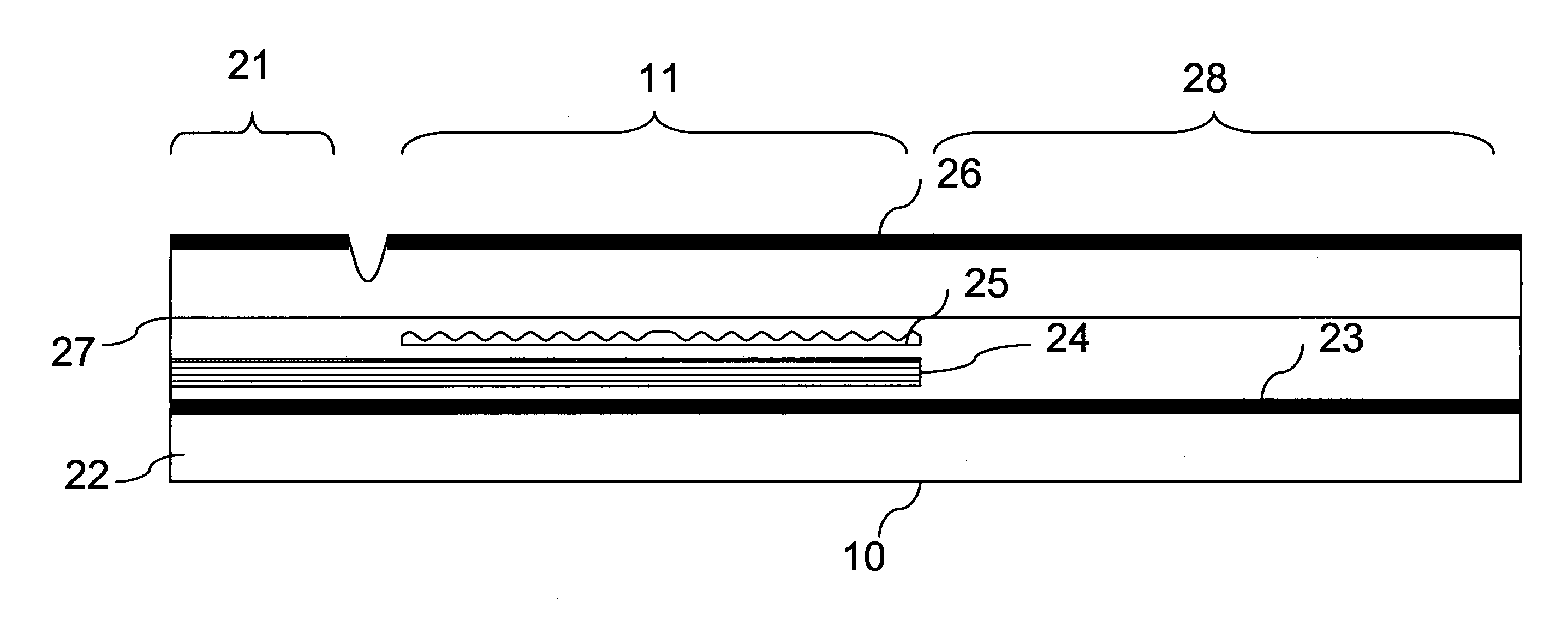
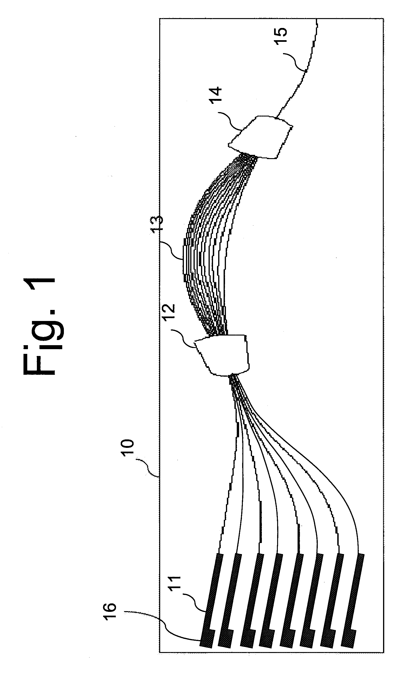
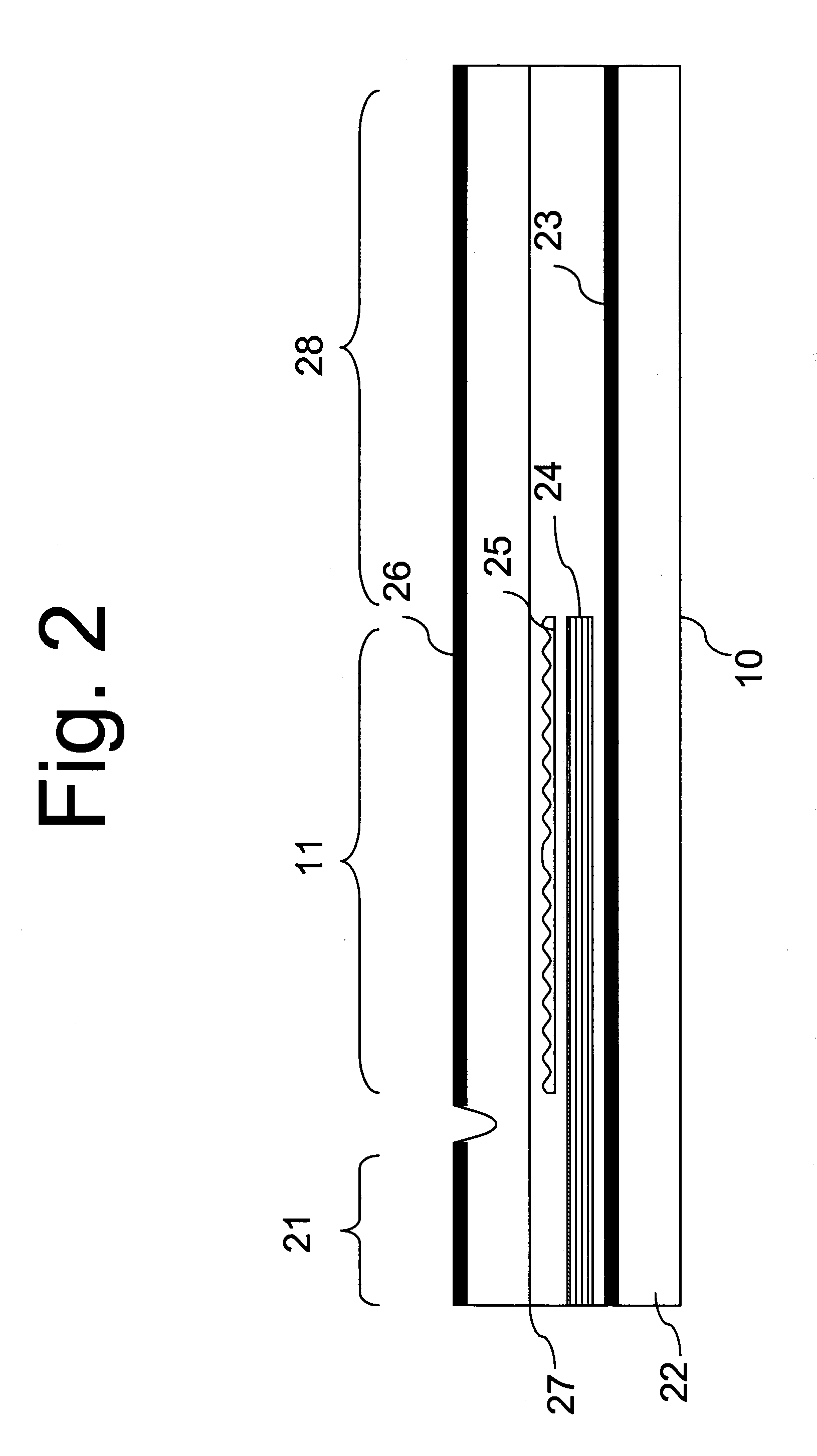
[0021]Reference is made to FIG. 1 illustrating an embodiment of a transmitter integrated circuit 10. A chip is made in InP semiconducting material and has 8 phase shifted DFB lasers 11. Each laser has a different grating pitch such that the wavelengths of the lasers are separated, preferably by 5 nm. The output of these lasers enters passive waveguides that contain no active region. These passive waveguide connect to an arrayed waveguide grating (AWG) (combination of 12, 13, 14) that multiplexes all the wavelengths of light together into a single output 15. The entire chip 10 can be made quite compact, since the wavelength spacing between the laser elements is large. In fact, the resolution of the AWG is dependent on the length difference between the arms, the wider laser wavelength spacing means a smaller AWG is possible.

[0022]The lasers are preferably directly modulated devices. In such embodiments each laser has a bond pad 16, that is connected to a driver source. Directly modula...


PUM


Abstract

Optical telecommunication modules including transmitters and receivers and methods of using same. In some embodiments the transmitters include a chip having an array of lasers and a combiner for combining light from the lasers for transmission over an optical fiber. Preferably the lasers have widely spaced wavelengths. The chip may be semi-cooled in some embodiments. A dither signal may be provided to one laser for use by a receiver in tracking temperature of the laser for improved receiver performance. In some embodiments a plurality of EMLs are used instead of a greater number of plurality of DFBs for transmission.

Description

CROSS-REFERENCE TO RELATED APPLICATION[0001]This application claims the benefit of U.S. Provisional Patent Application No. 60 / 782,432, filed Mar. 15, 2006, the disclosure of which is incorporated herein by reference.BACKGROUND OF INVENTION[0002]This invention relates generally to optical communications, and more particularly to optical telecommunication modules providing multiple modulated signals simultaneously from a single integrated device and receivers thereof.[0003]Telecommunication systems can be broadly divided into two separate domains. In the line-side, or long haul side, data are transferred long distances between local hubs, with optical amplification compensating for loss and dispersion compensating modules maintaining signal integrity. On the client side, or datacom side, on the other hand, the distances are generally, short such that optical amplification and dispersion compensation is not needed.[0004]Given the challenging requirements for transmitting signals thousa...

Claims


Application Information

Patent Timeline
IPC IPC(8): H04J14/02
CPCH04J14/02H01S5/4087H01S5/1039H01S5/0268H01S5/02415H01S5/0612H01S5/124H01S5/0264H01S5/00
Inventor PEZESHKI, BARDIA
Owner NEOPHOTONICS CORP
Why Eureka
Try Eureka