Protective wiring device

a protection device and wiring technology, applied in the direction of protective switch details, emergency protective arrangements for limiting excess voltage/current, instruments, etc., can solve the problems of easy damage to microprocessors or gfi detector chips, and easy short circuit failure of low voltage signal circuits. , to achieve the effect of reducing the surface area of the pcb, increasing the density of electronic components, and maintaining device reliability

Active Publication Date: 2016-09-06
PASS SEYMOUR
View PDF21 Cites 17 Cited by
  • Summary
  • Abstract
  • Description
  • Claims
  • Application Information

AI Technical Summary

Benefits of technology

[0013]The present invention addresses the needs described above by providing a protective device that substantially obviates the threat of surface tracking and cross-talk from high voltage components to signal voltage components while, at the same time, reducing the PCB surface area. Moreover, the present invention allows for an increase in the density of electronic components on a protective device PCB while maintaining device reliability. The present invention is also configured to substantially prevent voltage surges propagating in the AC electrical distribution system from damaging small signal components. In accomplishing the above stated objectives, the present invention also limits the number of conductive segments that comprise the AC conductive path from line to load to thus limit heat rise.
[0018]In another embodiment of the invention, the device also includes a separator portion disposed between the back body member and the front cover portion. The separator portion includes a reset pin aperture accessible via a first major surface facing the front cover and a reset pin guide portion disposed on an opposite second major surface facing the back body member. A latch block assembly includes a central latch block portion configured to accommodate a reset pin and a latching element. The central latch block portion includes an open side configured to accommodate the reset pin guide portion. The reset pin is substantially prevented from exiting the central latch block portion via the open side by the reset pin guide portion.
[0022]In another aspect, the present is directed to a protective device that includes a separator portion disposed between a back body member and a front cover portion. The separator portion includes a reset pin aperture accessible via a first major surface facing the front cover and a reset pin guide portion disposed on an opposite second major surface facing the back body member. The device further includes a latch block assembly having a central latch block portion configured to accommodate a reset pin and a latching element. The central latch block portion includes an open side configured to accommodate the reset pin guide portion. The reset pin is substantially prevented from exiting the central latch block portion via the open side by the reset pin guide portion.

Problems solved by technology

When electricity is allowed to track across the surface of a PCB, low voltage circuits may become short circuited and fail.
In addition, if unwanted electrical currents cause a device to over-heat, a fire could result.
As a result, the high circuit density noted above may result in AC voltage circuits being disposed next to, or proximate, a processor or other such low voltage circuits.
Accordingly, these delicate low voltage signal circuits may be subject to surface-tracking, cross-talk and / or voltage surges.
A 6 kV lightning surge, for example, could easily destroy a microprocessor or GFI detector chip.
Cross-talk can be an issue because it may affect the calibration of sensitive electrical circuits.
It is imperative that the detector can obtain a true reading on fault current readings because ground faults can result in human fatalities.
One can see, therefore, how large voltage noise signals can make small signal detections problematic.
However, this is a costly manufacturing process and it is subject to manufacturing variabilities.
While this approach can be effective, it also has drawbacks.
Another issue that is related to device reliability is heat-rise.
Devices must operate below a certain temperature or fire may result.
One of the main causes of heat-rise are the thermal losses (I2R) caused by resistive interconnections in the AC current path.

Method used


Image

  • Protective wiring device
  • Protective wiring device
  • Protective wiring device

Examples


Embodiment Construction

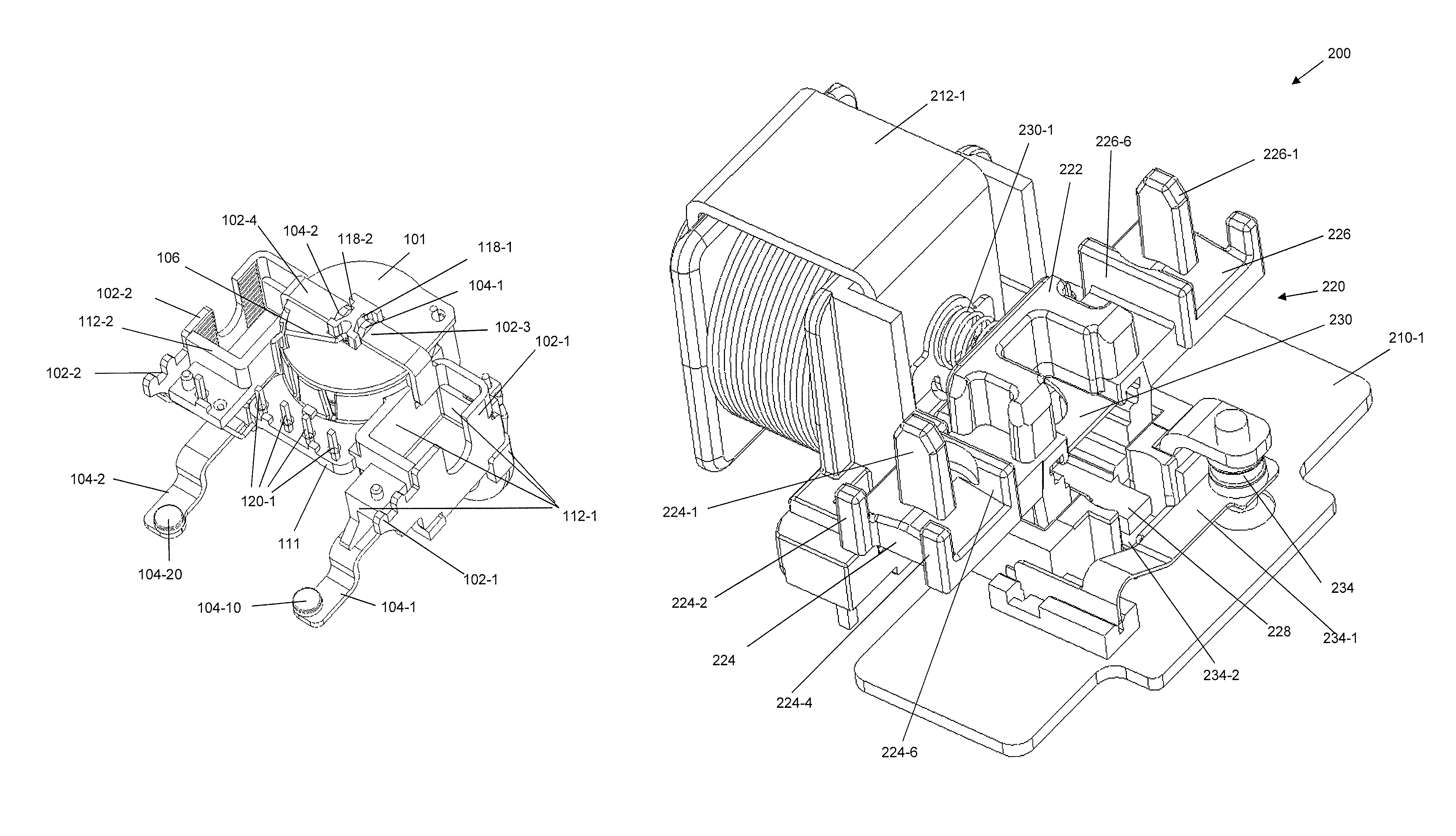
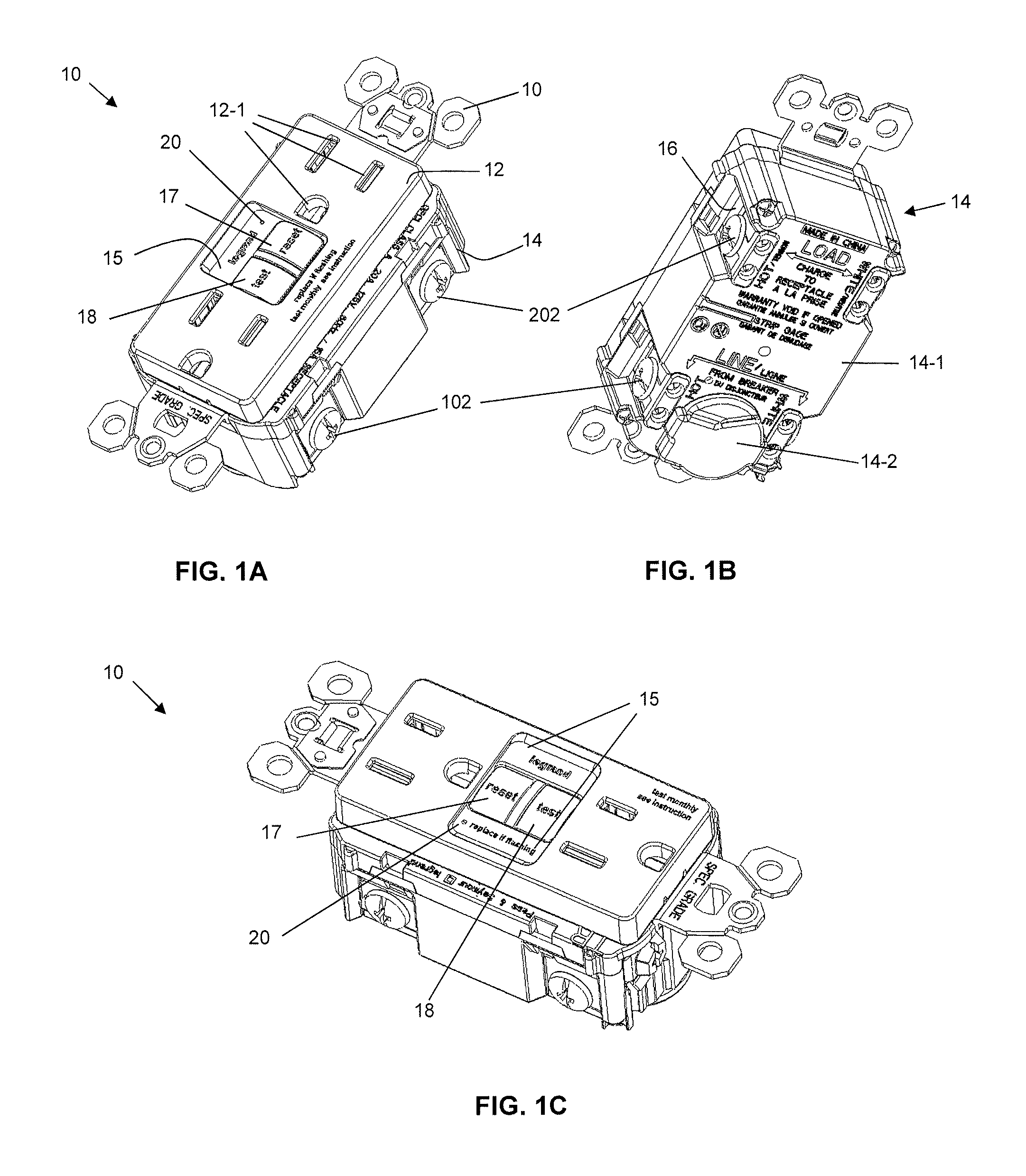
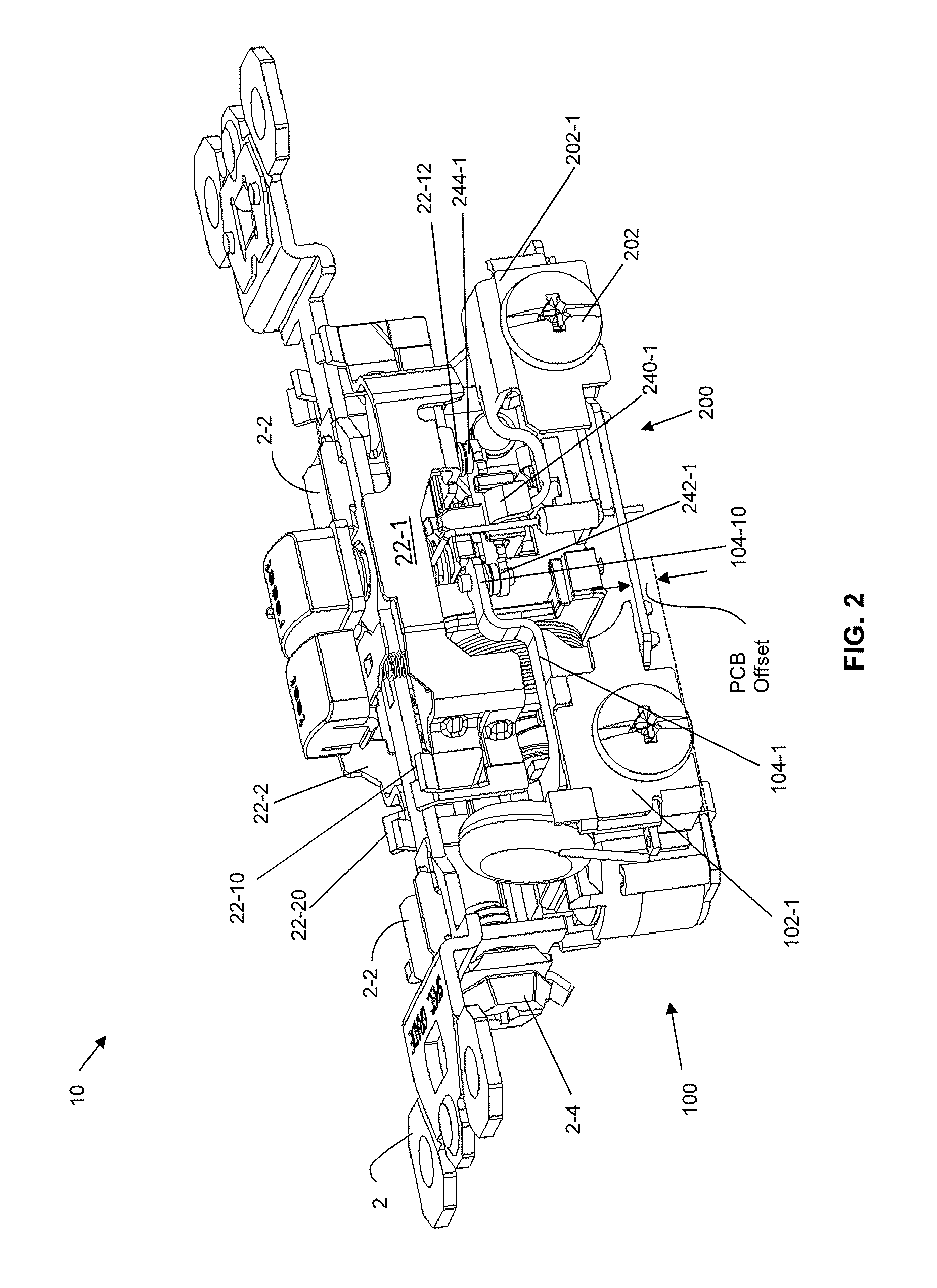
[0052]Reference will now be made in detail to the present exemplary embodiments of the invention, examples of which are illustrated in the accompanying drawings. Wherever possible, the same reference numbers will be used throughout the drawings to refer to the same or like parts. An exemplary embodiment of the protective device of the present invention is shown in FIGS. 1A-1C, and is designated generally throughout by reference numeral 10.

[0053]As embodied herein, and depicted in FIGS. 1A-1C, perspective views of the protective electrical wiring device in accordance with various embodiments of the present invention are disclosed. The protective device 10 includes a housing having a front cover 12, a back body member 14 and a separator 16. In these embodiments, only a small portion of the separator 16 can be viewed from the exterior of the device 10 (See, FIG. 1B). The front cover includes outlet receptacles 12-1 which are configured to accept the hot, neutral and ground blades of a ...


PUM


Abstract

The present is directed to a protective device that includes a separator portion disposed between a back body member and a front cover portion. The separator portion includes a reset pin aperture accessible via a first major surface facing the front cover and a reset pin guide portion disposed on an opposite second major surface facing the back body member. The device further includes a latch block assembly having a central latch block portion configured to accommodate a reset pin and a latching element. The central latch block portion includes an open side configured to accommodate the reset pin guide portion. The reset pin is substantially prevented from exiting the central latch block portion via the open side by the reset pin guide portion.

Description

BACKGROUND OF THE INVENTION[0001]1. Field of the Invention[0002]The present invention relates generally to electrical wiring devices, and particularly to protective wiring devices.[0003]2. Technical Background[0004]Electric circuits are installed throughout a structure such that electrical service is readily accessible to people that live or work in that structure. An electric circuit includes electrical wires that interconnect electrical wiring devices that are positioned at various locations throughout a structure. There are a variety of electrical wiring devices available to the consumer including outlet receptacles, light switches, dimmers, ground fault circuit interrupters, arc fault circuit interrupters and the like.[0005]Ground fault circuit interrupters (GFCIs), transient voltage surge suppressors (TVSS), surge protective devices (SPDs) and arc fault circuit interrupters (AFCIs) are examples of electrical protective devices. They are used to protect persons and structures fr...

Claims


Application Information

Patent Timeline
Patent Type & Authority Patents(United States)
IPC IPC(8): H01H83/02H02H3/10G01R31/02G01R15/18H02H3/00H02H3/06H02H9/04H01H83/04H02B13/00H01H71/02H01H83/22
CPCH01H83/02G01R15/18G01R31/025H01H83/04H02B13/00H02H3/00H02H3/06H02H3/105H02H9/04H01H71/0207H01H83/226G01R31/52H01H71/025
Inventor WEEKS, RICHARD
Owner PASS SEYMOUR
Why Eureka
Try Eureka