Low-power digital logic using a Boolean logic switched inductor-capacitor (SLC) circuit

a low-power, digital logic technology, applied in logic circuits, logic circuits characterised by logic functions, pulse techniques, etc., can solve the problems of sacrificing switching speed, allowing quadratic power reduction, and reducing storage energy, so as to prevent oscillation, reduce leakage, and reduce the effect of stored energy

Active Publication Date: 2016-09-06
RAYTHEON CO
View PDF2 Cites 11 Cited by
  • Summary
  • Abstract
  • Description
  • Claims
  • Application Information

AI Technical Summary

Benefits of technology

[0018]In non-ideal devices, stored energy is reduced through leakage current or dissipated on path resistance. In different embodiments, a recharge circuit is used to provide a ground reference at the bottom the capacitor to recharge the logical output at the top of the capacitor. First and second recharge circuits are coupled to the top and bottom of the load capacitor, respectively. The recharge circuits are suitably “pulsed” to provide the ground reference for a period of time sufficient to recharge the logical output and remaining floating otherwise to reduce leakage.
[0019]In an embodiment, a low-power digital logic circuit comprises first and second pass-through logic (PTL) cells that each implements the same Boolean logic. Each cell has a logical input, a bias input and first and second parallel outputs configured to switch in opposition. An inductor is coupled between the bias inputs of the first and second PTL cells. A first unidirectional switch is coupled between the second output of the first PTL cell and a logical output at the top of a load capacitor. When enabled the first unidirectional switch allows the inductor to pull charge from the bottom of the capacitor through the inductor to the top of the load capacitor to switch a logic level 1 at the logic output. The first unidirectional switch traps charge on the top of the capacitor to hold the logic level 1 and prevent oscillation. A second unidirectional switch is coupled between the first output of the second PTL cell and the bottom of the load capacitor. When enabled the second unidirectional switch allows the inductor to pull charge from the top of the capacitor through the inductor to the bottom of the load capacitor to switch a logic level 0 at the logical output. The second unidirectional switch traps charge on the bottom of the capacitor to hold the logic level 0 and prevent oscillation.

Problems solved by technology

Power dissipation in a CMOS based logic circuit is attributable to leakage current, short circuit current and switching energy.
Switching energy is more problematic.
This approach only allows quadratic reductions in power and sacrifices switching speed.

Method used


Image

  • Low-power digital logic using a Boolean logic switched inductor-capacitor (SLC) circuit
  • Low-power digital logic using a Boolean logic switched inductor-capacitor (SLC) circuit
  • Low-power digital logic using a Boolean logic switched inductor-capacitor (SLC) circuit

Examples


Embodiment Construction

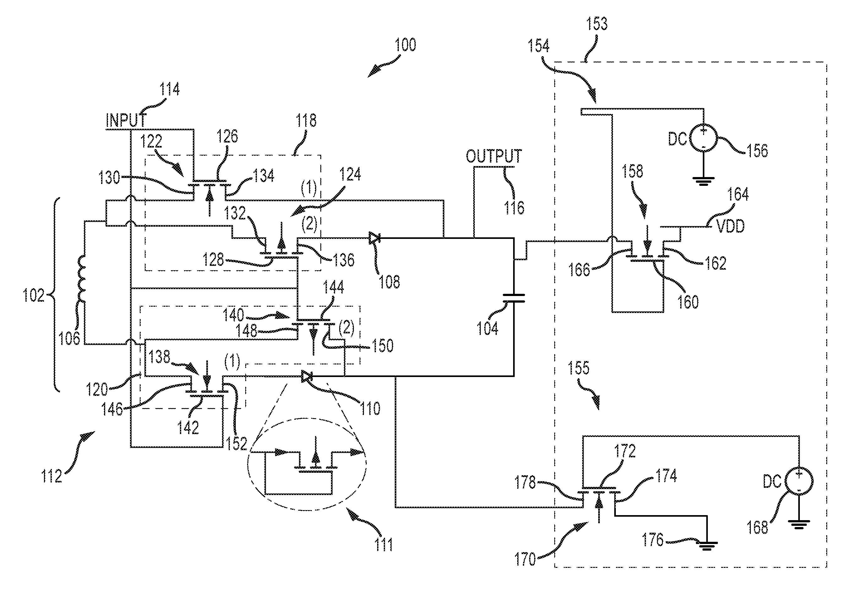
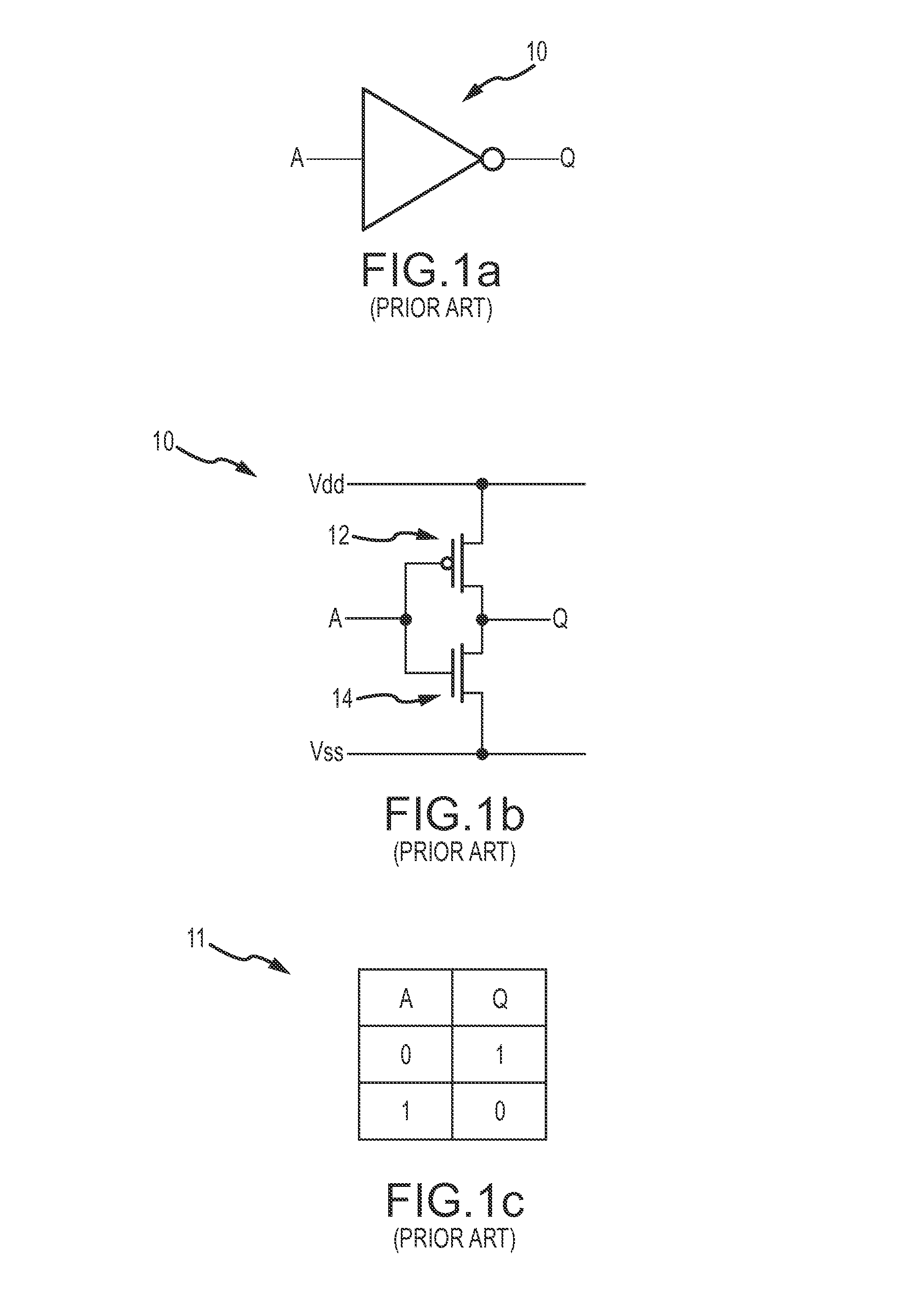
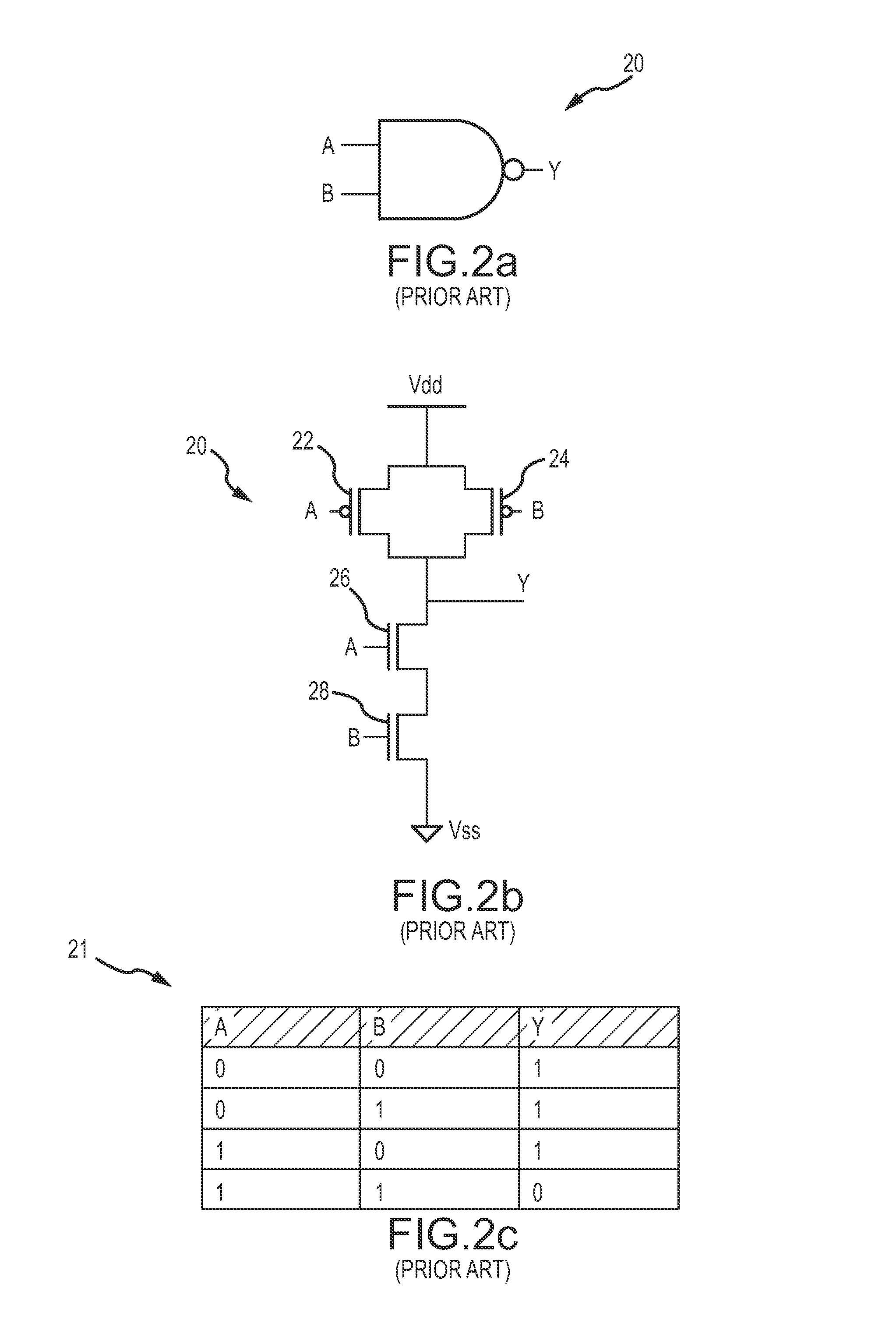
[0028]A goal of a low-power architecture for digital logic is to exhibit the same logic and voltage level behavior as the standard digital logic. The exact same logic inputs and logical outputs should characterize the low-power digital logic. Moreover, similar voltage levels should be created at the logical output. To achieve lower power, the architecture may have different internal physical characteristics and switching speeds.

[0029]Starzyk's low power logic circuit design scheme based on a SLC circuit does not exhibit the same logical behavior as standard CMOS gates. Specifically, two control signals CS1 and CS2 are used to control four switches. The use of two control signals CS1 and CS2 and the manner in which they are used is not consistent with standard input logic.

[0030]The present invention provides low-power digital logic that exhibits the same logic and voltage level behavior as standard digital logic. The low-power digital logic uses a logic switch and a pair of unidirect...


PUM


Abstract

A low-power digital logic architecture exhibits the same logic and voltage level behavior as standard digital logic. A logic switch and a pair of unidirectional switches are used to control the direction of charge flow in a switched-inductor capacitor (SLC) circuit, allowing the inductor to pull charge back-and-forth from one side of the load capacitor to the other to both switch the logical state at the top of the capacitor and to recycle and store the charge in the capacitor itself.

Description

BACKGROUND OF THE INVENTION[0001]1. Field of the Invention[0002]This invention relates to digital logic, and more particularly to a new low-power architecture for digital logic that uses a switched inductor-capacitor (SLC) circuit to recycle charge while exhibiting the same logic behavior as standard digital logic.[0003]2. Description of the Related Art[0004]A logic gate is an idealized or physical device that implements a Boolean function. The logic gate performs a logical operation on one or more logical inputs, and produces a single logical output. Typical logic gates include “AND”, “OR”, “INVERTER”, “NAND”, “NOR”, “XOR” and “XNOR”. These logic gates are combined to design arbitrary digital logic circuits.[0005]There are several logic families with different characteristics (power consumption, speed, cost, size) such as: RDL (resistor-diode logic), RTL (resistor-transistor logic), DTL (diode-transistor logic), TTL (transistor-transistor logic) and CMOS (complementary metal oxide ...

Claims


Application Information

Patent Timeline
Patent Type & Authority Patents(United States)
IPC IPC(8): H03K19/20H03K19/00H03K19/094H03K19/08
CPCH03K19/0013H03K19/0806
Inventor MARR, HARRY B.PRAGER, KENNETH E.KARL, JULIA L.THOMPSON, DANIEL
Owner RAYTHEON CO
Why Eureka
Try Eureka