Method for directly attaching dielectric to circuit board with embedded electronic devices

Active Publication Date: 2016-09-13
UNITECH PRINTED CIRCUIT BOARD CORP
View PDF4 Cites 5 Cited by
  • Summary
  • Abstract
  • Description
  • Claims
  • Application Information

AI Technical Summary

Benefits of technology

The present invention provides a method for directly attaching dielectric to a circuit board with embedded electronic devices. This is done by creating multiple through holes that correspond to the electrodes of the electronic device. This ensures accurate positioning of the electrodes during the embedding process. By using an adhesive first dielectric layer, the electronic device is directly stuck on the layer, saving money on adhesive material or metal conductive paste.

Problems solved by technology

In the field of PCB, area occupied by electronic components is always a restriction for approaching slim volume, and there is one more important issue that excessive welding points cause lower reliability and increasing cost.
Further, adhesive material or metal conductive paste may be applied to those electronic components in order to stick electronic components onto a dielectric layer, and it causes higher manufacturing cost.

Method used


Image

  • Method for directly attaching dielectric to circuit board with embedded electronic devices
  • Method for directly attaching dielectric to circuit board with embedded electronic devices
  • Method for directly attaching dielectric to circuit board with embedded electronic devices

Examples


Embodiment Construction

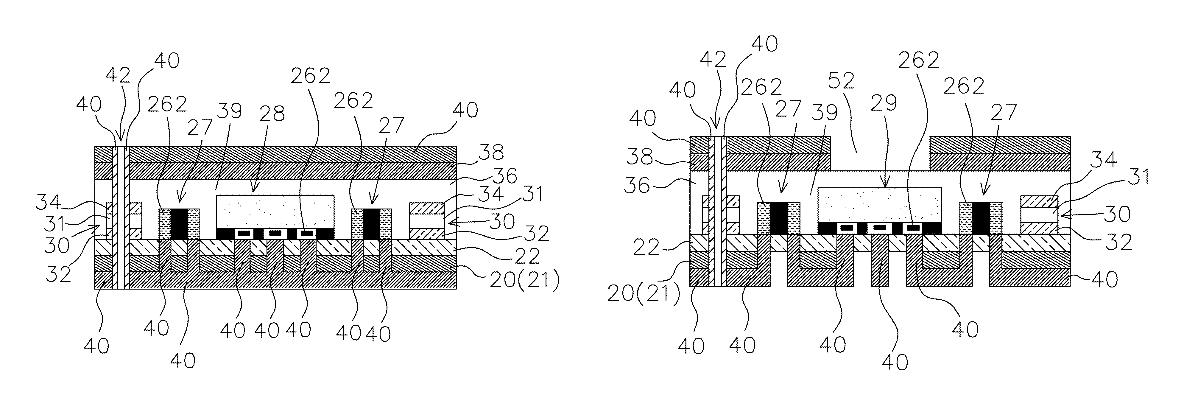
[0029]Following preferred embodiments and figures will be described in detail so as to achieve aforesaid objects.

[0030]Please refer to FIG. 1 to FIG. 6, which disclose a method for directly attaching dielectric to a circuit board with embedded electronic devices, and the method comprises the steps of:

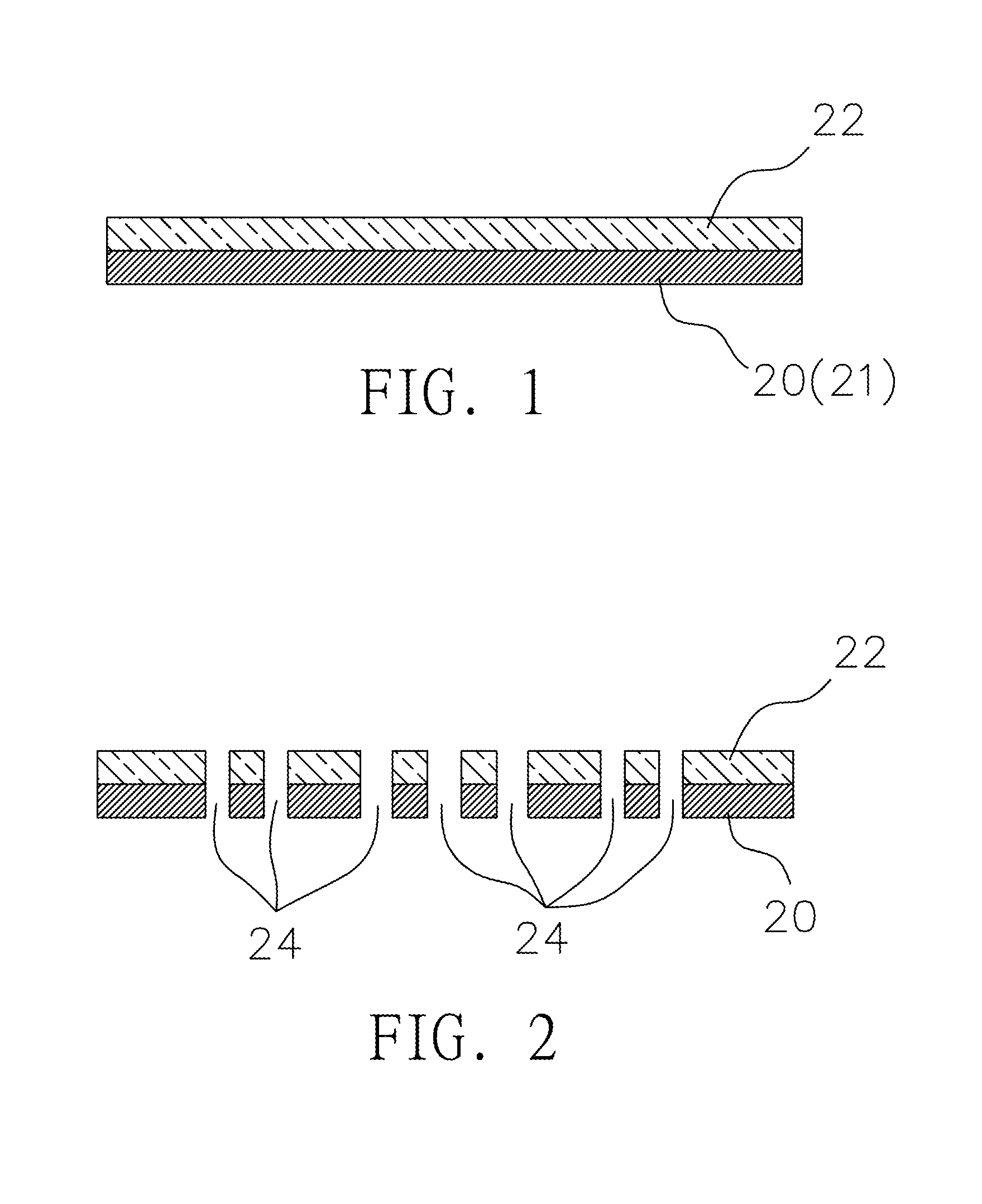
[0031]providing a copper clad laminate 20 that comprises a copper layer, as shown in FIG. 1; attaching a first dielectric layer 22 to the copper clad laminate 20, wherein the first dielectric layer 22 is adhesive; wherein the copper clad laminate 20 has a first circuit layer 21 beyond, the first circuit layer 21 is built for circuits via film, exposure, development, etching;

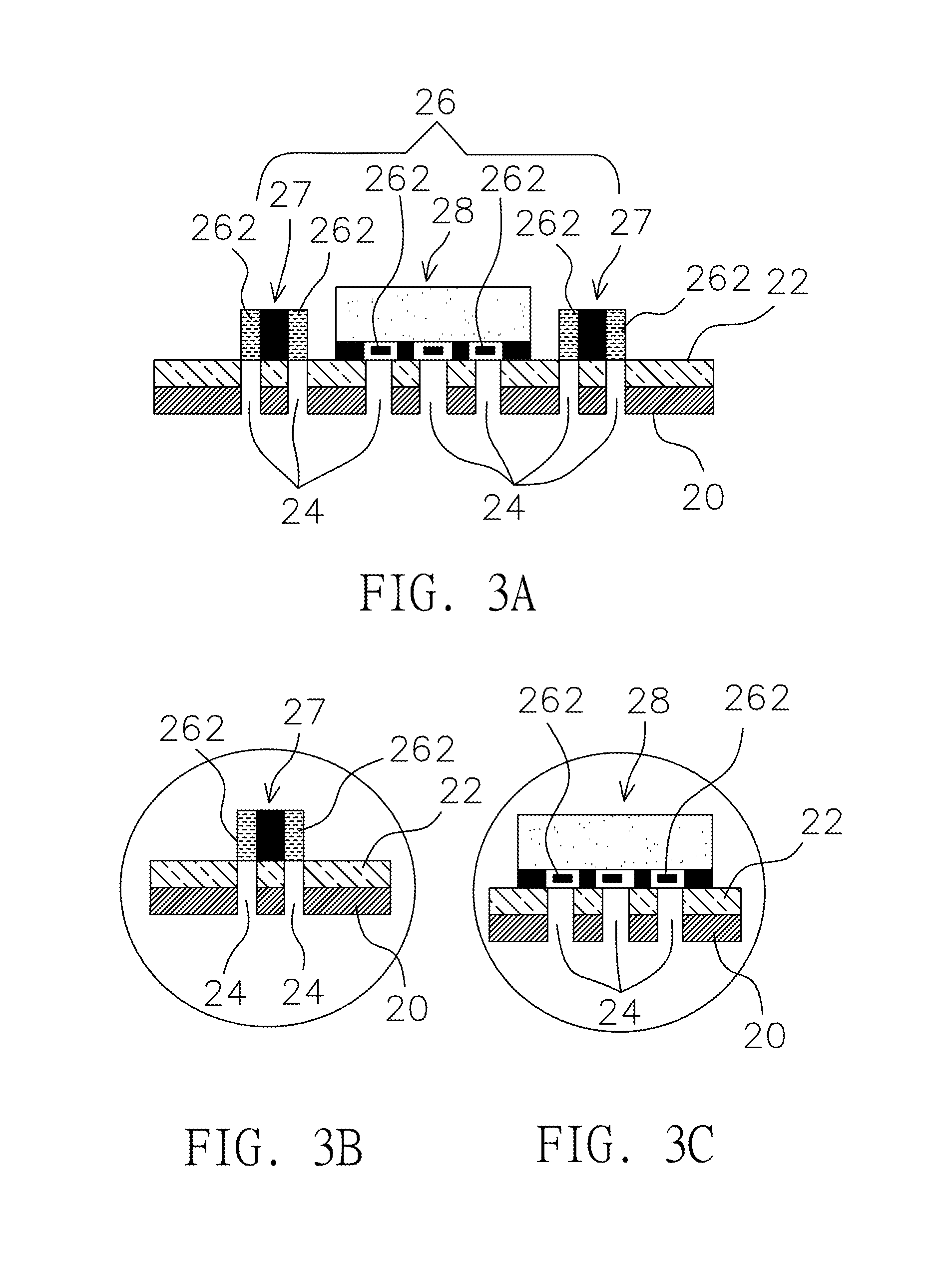
[0032]producing a plurality of through holes 24 in the first dielectric layer 22 and the copper clad laminate 20, as shown in FIG. 2, the through holes 24 being corresponding to the plural electrodes 262 of at least one electronic device 26 as shown in FIG. 3A, wherein the electronic device 26 pre-sets in the first d...


PUM


Abstract

A method for directly attaching dielectric to a circuit board with embedded electronic devices is provided. That is, a plurality of through holes are produced before embedding an electronic device, wherein plural through holes are corresponding to a plurality of electrodes of the electronic device. So that the plural electrodes of the electronic device is accurately positioned with the through holes if the electronic device is being embedded. On the other hand, since the first dielectric layer is adhesive, the electronic device is directly stuck on the first dielectric layer in order to save cost of adhesive material or metal conductive paste in prior arts.

Description

BACKGROUND OF THE INVENTION[0001]1. Field of the Invention[0002]The present invention generally relates to a method for manufacturing a PCB, more particularly to a method for directly attaching dielectric to a circuit board with embedded electronic devices.[0003]2. Description of the Prior Art[0004]Fast and high-density, the two requirements have been the driving forces in the field of high-tech development. Those purposes are to reduce production costs and to meet consumer demand. Therefore, nowadays, electronics and mobile communications products are continuously approaching slim volume, versatility, high reliability and cost reduction with a generation rate of three to five years. Accordingly, for the IC design of electronic products, electronic components occupying largest areas are undertaking an integration of the revolution.[0005]In the field of PCB, area occupied by electronic components is always a restriction for approaching slim volume, and there is one more important iss...

Claims


Application Information

Patent Timeline
IPC IPC(8): H01L21/00H01L33/52H01L33/48H01L33/62H01L21/48
CPCH01L21/486H01L33/486H01L33/62H01L21/4857H01L33/52H01L2933/0066H01L2933/005H01L23/49827H01L23/5389H01L24/24H01L24/82H01L2224/04105H01L2224/24195H01L2224/92144H01L2924/19041H01L2924/19042H01L2924/19043H01L2924/19105H01L2924/12041H01L25/167H05K2201/10674H05K2203/063H05K2201/10106H05K1/188H05K2201/10636Y02P70/50
Inventor YEH, MING YIHSU, SHUN YUEHCHEN, KUN CHICHEN, HUNG MIN
Owner UNITECH PRINTED CIRCUIT BOARD CORP
Why Eureka
Try Eureka