

Low-oxidation plasma-assisted process
a plasma-assisted, low-oxidation technology, applied in the direction of chemical vapor deposition coating, coating, electric discharge tube, etc., can solve the problems of low rf power, problems to be solved, etc., to suppress oxidation of an underlying layer, good film quality
- Summary
- Abstract
- Description
- Claims
- Application Information
AI Technical Summary
Benefits of technology
Problems solved by technology
Method used
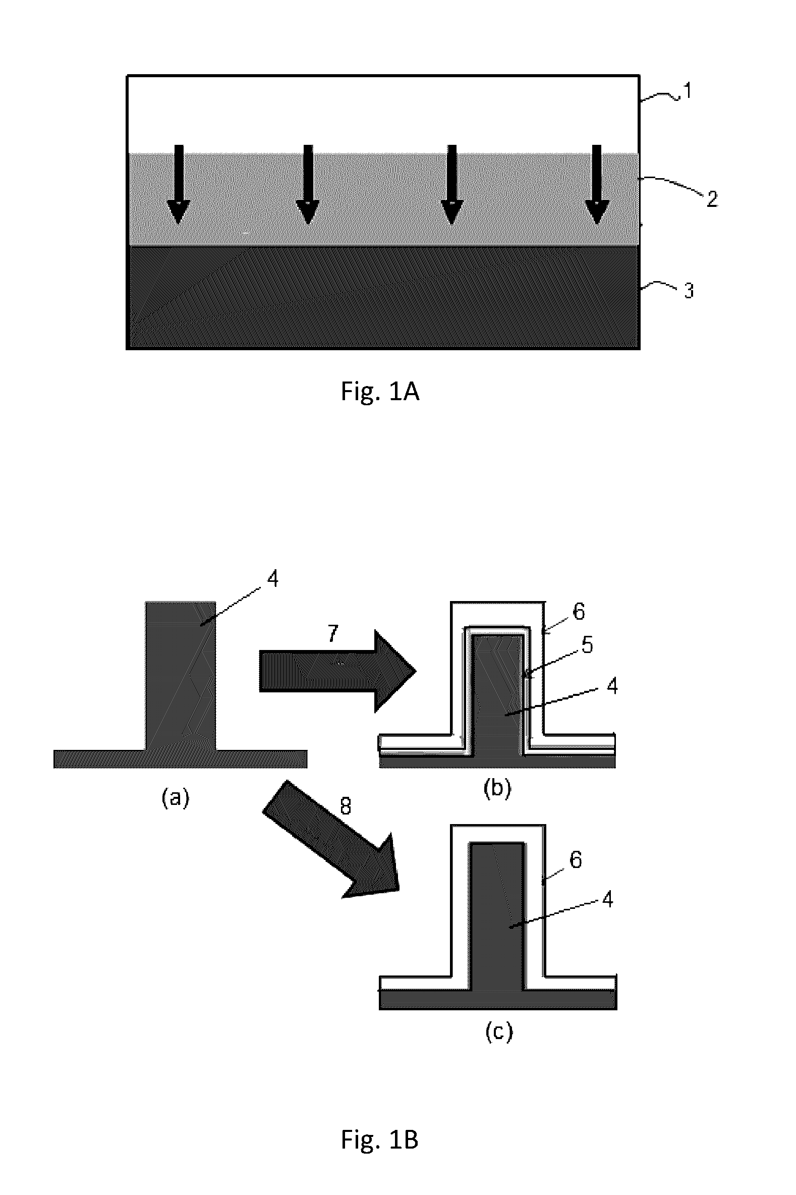
Image

Examples
example 1
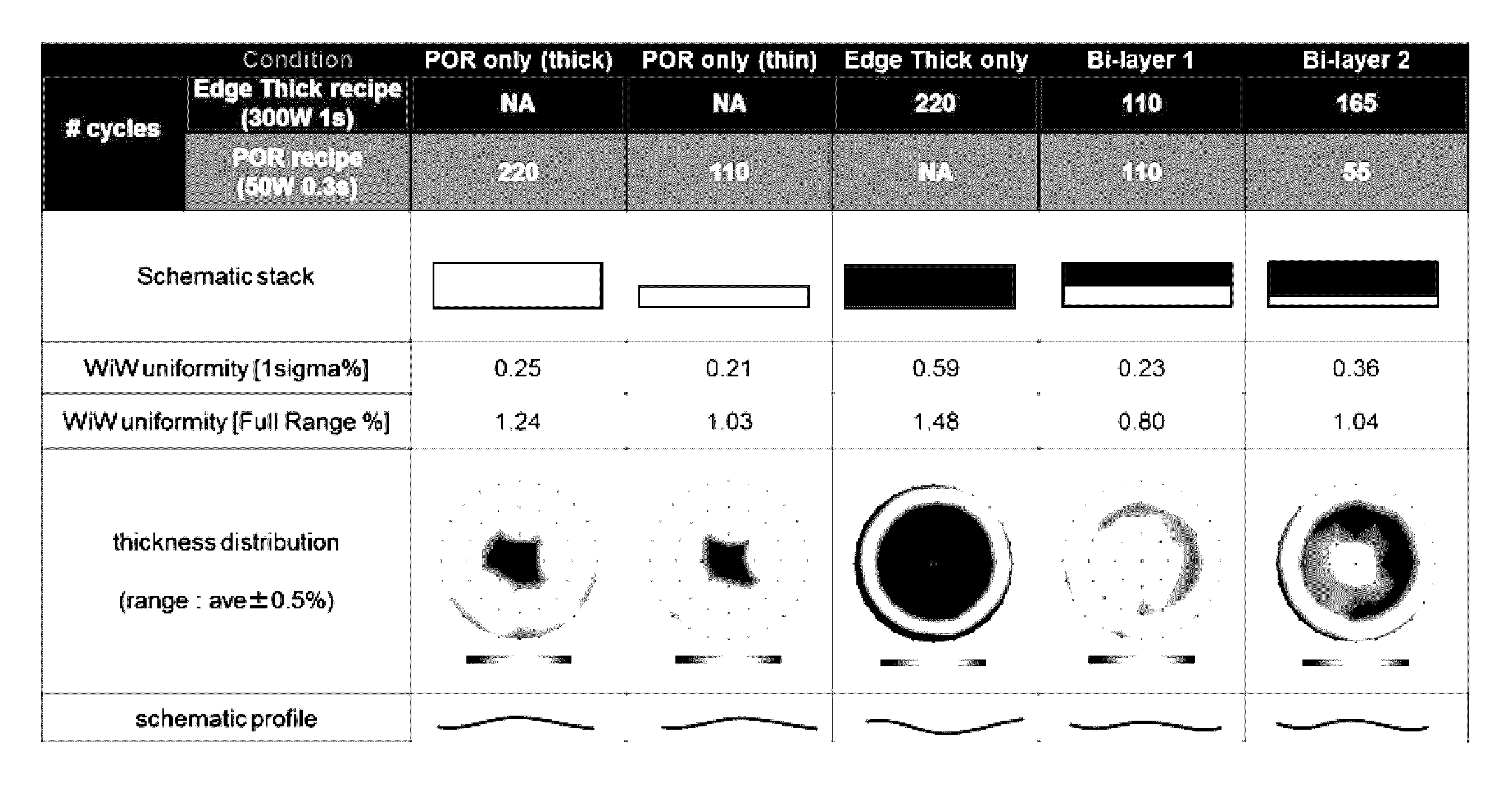
[0060]A 300-mm Si substrate having a photoresist pattern formed thereon was loaded in an apparatus illustrated in FIG. 6 and an oxide film was deposited by PEALD under conditions shown in Table 5 below. The results are shown in FIG. 2A. In this application, a target film was required to have a film profile showing a relatively high thickness along the periphery of the substrate. In the table, the term “POR only (thick)” (“POR” refers to “process of reference film—Center Thick”) refers to a PEALD process using low-RF power oxygen plasma only, until a thickness of a film reached about 20 nm. The term “POR only (thin)” refers to a PEALD process using low-RF power oxygen plasma only, until the thickness of a film reached about 10 nm. The term “Edge Thick only” refers to a PEALD process using high-RF power oxygen plasma only, until the thickness of a film reached about 20 nm. The term “Bi-layer 1” refers to a PEALD process using low-RF power oxygen plasma until the thickness of a film re...
example 2
[0067]Oxide films were deposited on substrates by PEALD under conditions shown in Table 7 below using the apparatus illustrated in FIG. 6. The “Low Power SiO” refers to a SiO film deposited using the X cycles with low RF power in shown in FIG. 4. The “High Power SiO” refers to a SiO film deposited using the X cycles with high RF power in place of low RF power shown in FIG. 4 (modified X cycles). The “Low Power HQ SiO” refers to a SiO film deposited using the Z cycles which include the X cycles and the Y cycles shown in FIG. 4. The resultant films were subjected to a wet etching test.
[0068]
TABLE 7Low PowerLowHighHQ SiOConditionsPower SiOPower SiOXYPrecursorBDEASBDEASBDEASN / APrecursor[deg C.]50505050Bottle TempCarrier Ar[sccm]2000200020002000O2[sccm]400040003000N / ASeal He[sccm]20020018001800RC Press[Pa]400400333333HRF[W]100500100500SUS temp[deg C.]7575300300SHD temp[deg C.]7575150150Wall Temp[deg C.]7575130130Gap[mm]7.57.57.57.5CycleSource-Feed0.20.20.2N / ATimeSource-Purge0.30.30.3N / A[...
PUM
| Property | Measurement | Unit |
|---|---|---|
| thickness | aaaaa | aaaaa |
| thickness | aaaaa | aaaaa |
| time | aaaaa | aaaaa |
Abstract
Description
Claims
Application Information