Long wavelength indium arsenide phosphide (InAsP) quantum well active region and method for producing same

Inactive Publication Date: 2007-10-02
AVAGO TECH WIRELESS IP SINGAPORE PTE
View PDF4 Cites 0 Cited by
  • Summary
  • Abstract
  • Description
  • Claims
  • Application Information

AI Technical Summary

Benefits of technology

[0010]Embodiments of the invention provide several methods for using OMVPE to grow high quality, long wavelength light emitting active regions. In one embodiment, the invention is a method for producing an active region for a long wavelength light emitting device, comprising placing a substrate in an organometallic vapor phase epitaxy (OMVPE) reactor, the substrate for supporting growth of an indium ars

Problems solved by technology

Unfortunately, for a conventional light emitting device having an InGaAsP quantum well layer, the value of T0 is small, resulting in a rapid increase in the value of Ith when temperature rises.
Therefore, InGaAsP quantum well layers are not particularly well suited for 1.5 μm wavelength output light emitting devices in which a low threshold current and high characteristic temperature are desired.
Unfortunately, when using conventional processing techniques, such an arsenic fraction results in a significant lattice mismatch when the InAsP is grown over InP.
These highly strained quantum well layers may relax during, or after their formation, thereby resulting

Method used


Image

  • Long wavelength indium arsenide phosphide (InAsP) quantum well active region and method for producing same
  • Long wavelength indium arsenide phosphide (InAsP) quantum well active region and method for producing same
  • Long wavelength indium arsenide phosphide (InAsP) quantum well active region and method for producing same

Examples


Example

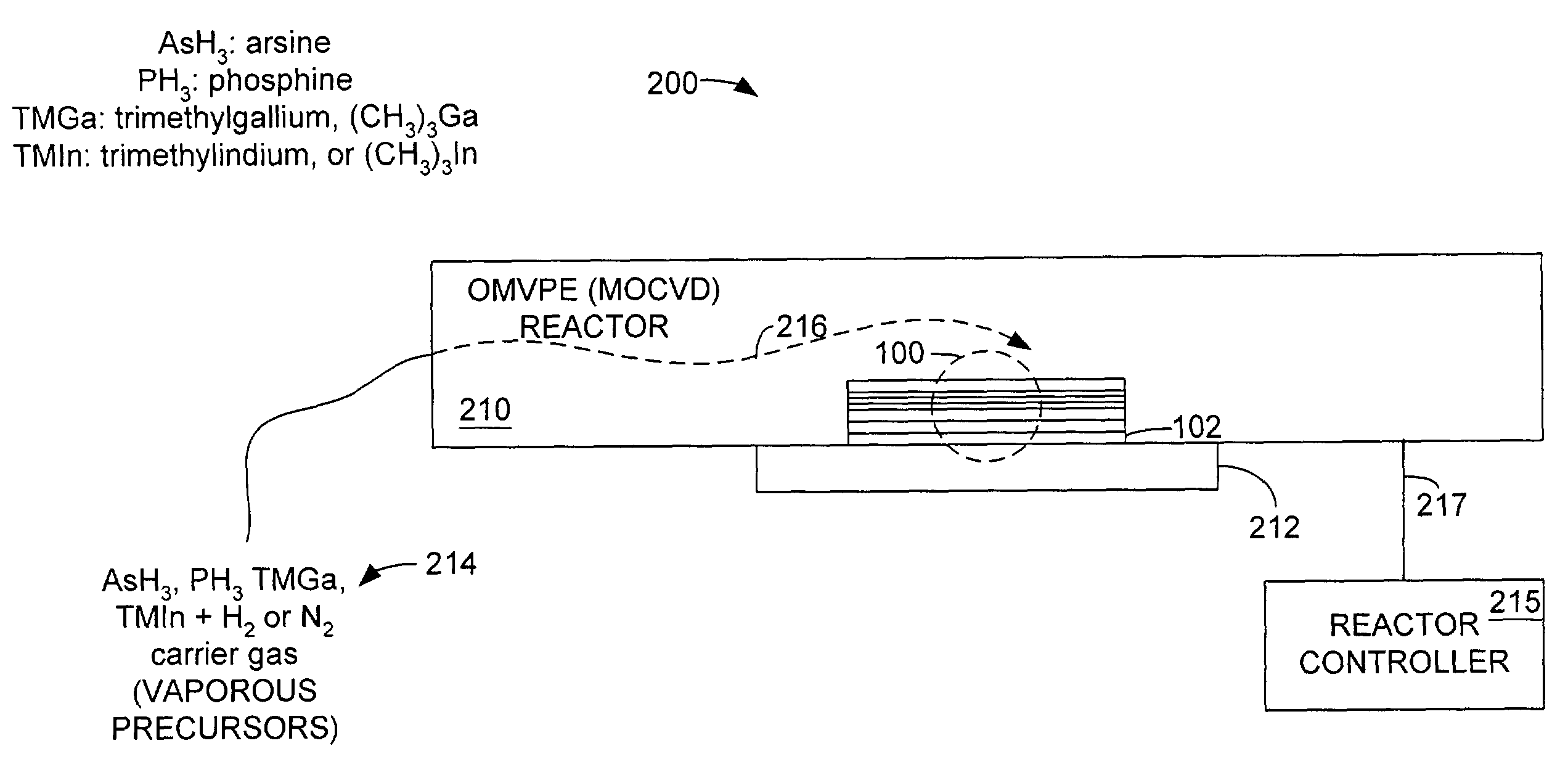
[0020]While described below using an example of an edge emitting laser that incorporates InAsP quantum well layers, other device structures can benefit from the invention. For example, a vertical-cavity surface-emitting laser (VCSEL) including high quality InAsP quantum well epitaxial layers can be economically fabricated using the concepts of the invention.

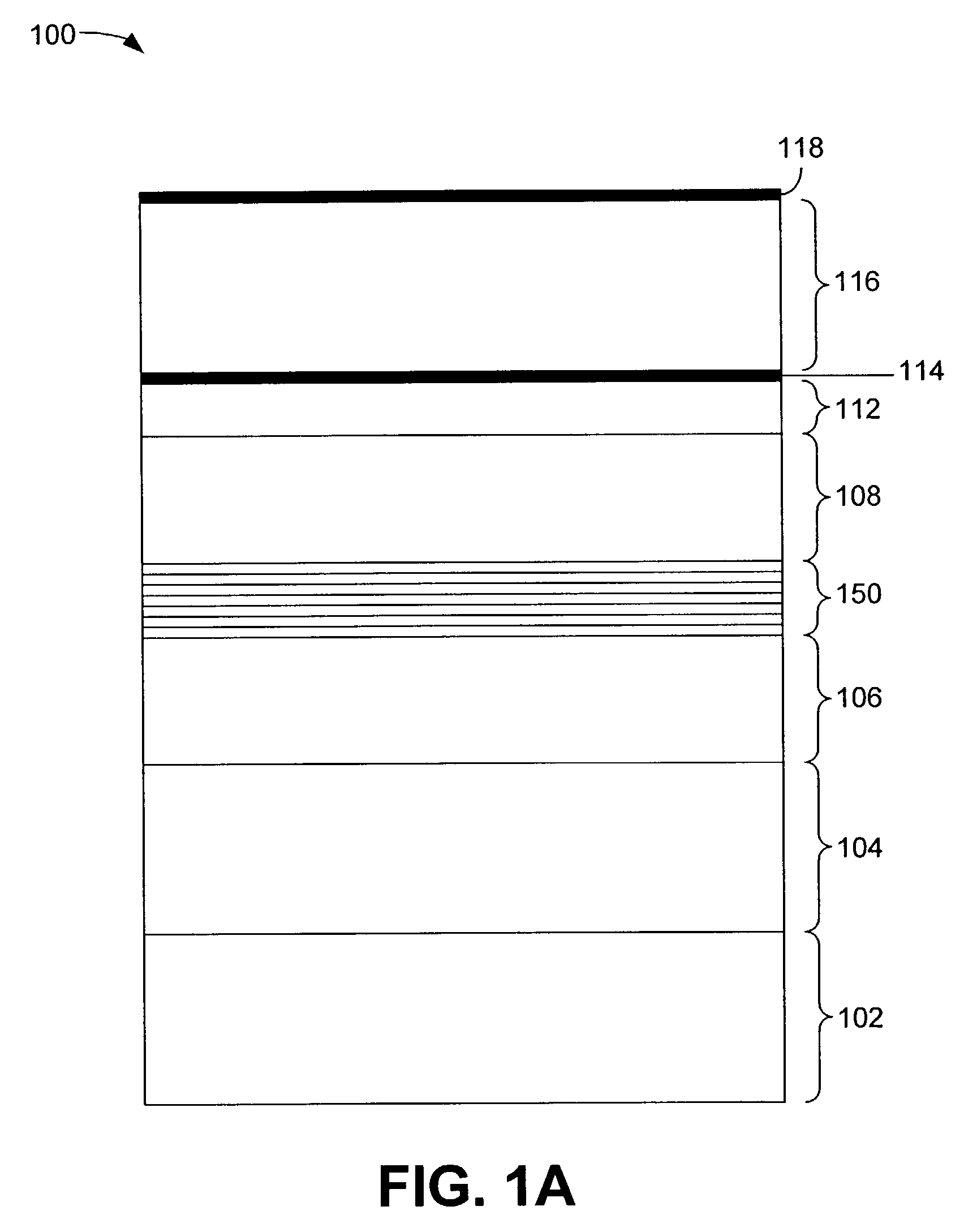
[0021]FIG. 1A is a schematic view illustrating the relevant portions of an exemplary edge emitting laser 100 constructed in accordance with an aspect of the invention. Some of the elements of the laser 100 are omitted for simplicity. The laser 100 comprises an N-type, sulfur (S) doped, indium phosphide (InP) substrate 102 over which an n-type 2 μm thick, selenium (Se) doped, InP cladding layer 104 is formed. The cladding layer 104 is formed using a high bandgap, low refractive index material.

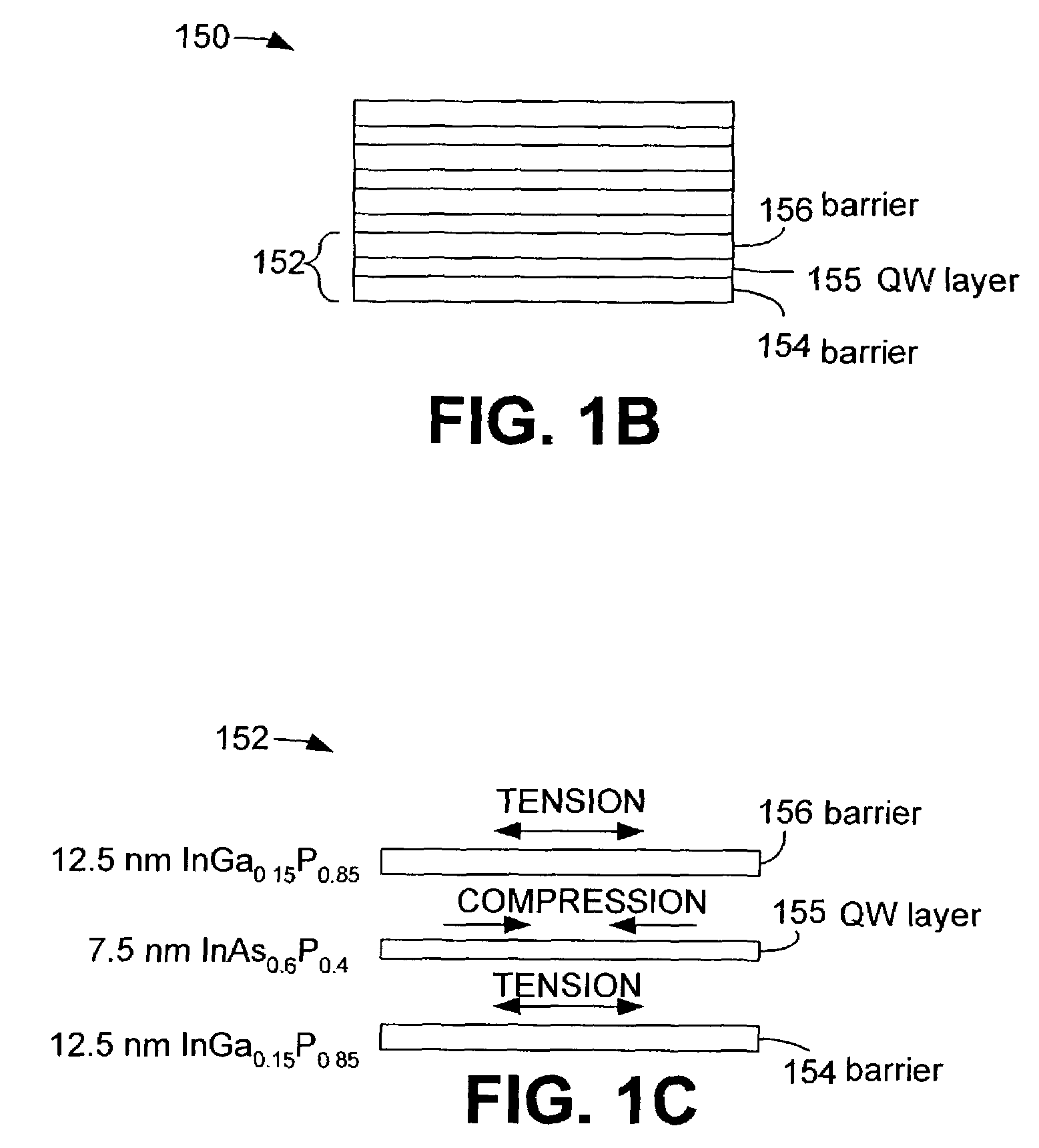
[0022]A lower separate confinement heterostructure (SCH) layer 106 is formed over the cladding layer 104. The lower SCH layer 106 is prefera...


PUM


Abstract

An InAsP active region for a long wavelength light emitting device and a method for growing the same are disclosed. In one embodiment, the method comprises placing a substrate in an organometallic vapor phase epitaxy (OMVPE) reactor, the substrate for supporting growth of an indium arsenide phosphide (InAsP) film, forming a quantum well layer of InAsP, and forming a barrier layer adjacent the quantum well layer, where the quantum well layer and the barrier layer are formed at a temperature of less than 520 degrees C. Forming the quantum well layer and the barrier layer at a temperature of less than 520 degrees C. results in fewer dislocations by suppressing relaxation of the layers. A long wavelength active region including InAsP quantum well layers and InGaP barrier layers is also disclosed.

Description

TECHNICAL FIELD[0001]The invention relates generally to light emitting devices, and, more particularly, to an indium arsenide phosphide (InAsP) quantum well active region for a long wavelength light emitting device and a method for producing same.BACKGROUND OF THE INVENTION[0002]Light emitting devices are used in many applications including optical communication systems. Optical communication systems have been in existence for some time and continue to increase in use due to the large amount of bandwidth available for transporting signals. Optical communication systems provide high bandwidth and superior speed and are suitable for efficiently communicating large amounts of voice and data over long distances. Optical communication systems that operate at relatively long wavelengths on the order of 1.3 micrometers (μm) to 1.55 μm are generally preferred because optical fibers generally have their lowest attenuation in this wavelength range. These long wavelength optical communication ...

Claims


Application Information

Patent Timeline
IPC IPC(8): H01L21/205H01L21/20H01L33/00H01S5/343
CPCB82Y20/00H01L21/02461H01L21/02463H01L21/02507H01L21/02546H01L21/0262H01L33/0062H01L21/02543H01S5/3434
Inventor BOUR, DAVID P.TAN, MICHAEL R. T.PEREZ, WILLIAM H.
Owner AVAGO TECH WIRELESS IP SINGAPORE PTE
Why Eureka
Try Eureka