

Method of manufacturing Group III nitride substrate and semiconductor device
- Summary
- Abstract
- Description
- Claims
- Application Information
AI Technical Summary
Benefits of technology
Problems solved by technology
Method used
Image

Examples
embodiment 1
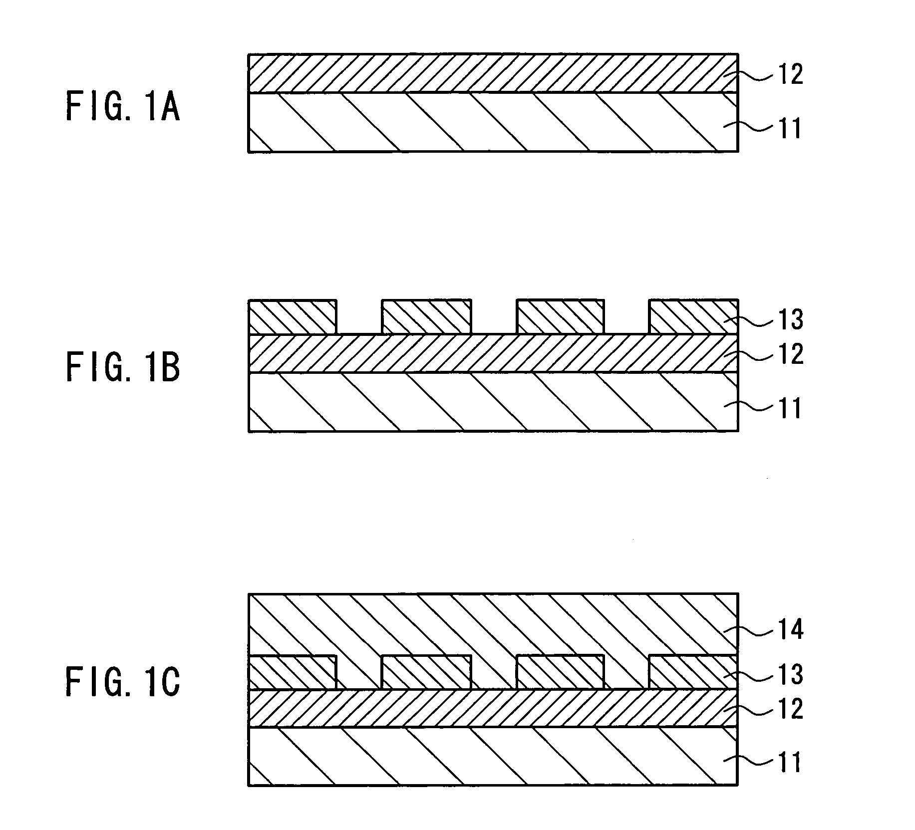
[0062]An example of the first manufacturing method of the present invention for manufacturing a Group III nitride substrate is described below with reference to FIGS. 1A to 1C.
[0063]FIGS. 1A to 1C are cross-sectional views showing an example of steps of the first manufacturing method according to the present invention. First a semiconductor layer 12 that is expressed by a composition formula of AluGavIn1−u−vN (where 0≦u≦1, 0≦v≦1, and u+v≦1) is prepared (step (i)). On this step, for example, the semiconductor layer 12 is formed on a base substrate 11, as shown in FIG. 1A. The semiconductor layer 12 can be formed by, for instance, a metalorganic chemical vapor deposition (MOCVD) method, a molecular beam epitaxy (MBE) method, or a hydride vapor phase epitaxy (HVPE) method. The base substrate 11 can be, for example, a sapphire substrate, a GaAs substrate, a Si substrate, a SiC substrate, or a AlN substrate. The sapphire substrate can be, for instance, a sapphire substrate whose surface ...
embodiment 2
[0074]Next, an example of the second manufacturing method of the present invention for manufacturing a Group III nitride substrate is described with reference to FIGS. 3A to 3C.
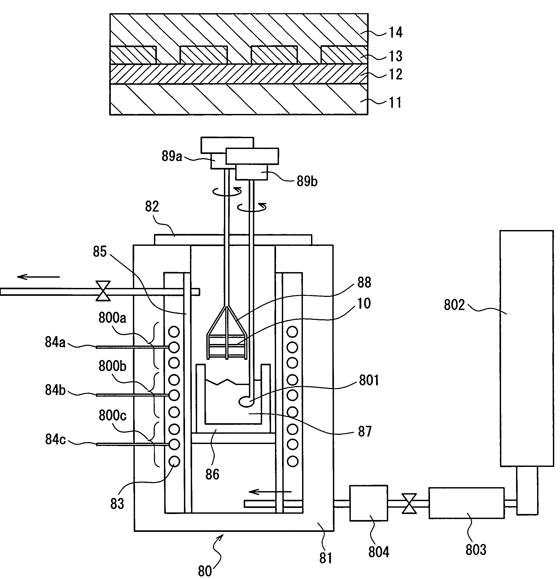
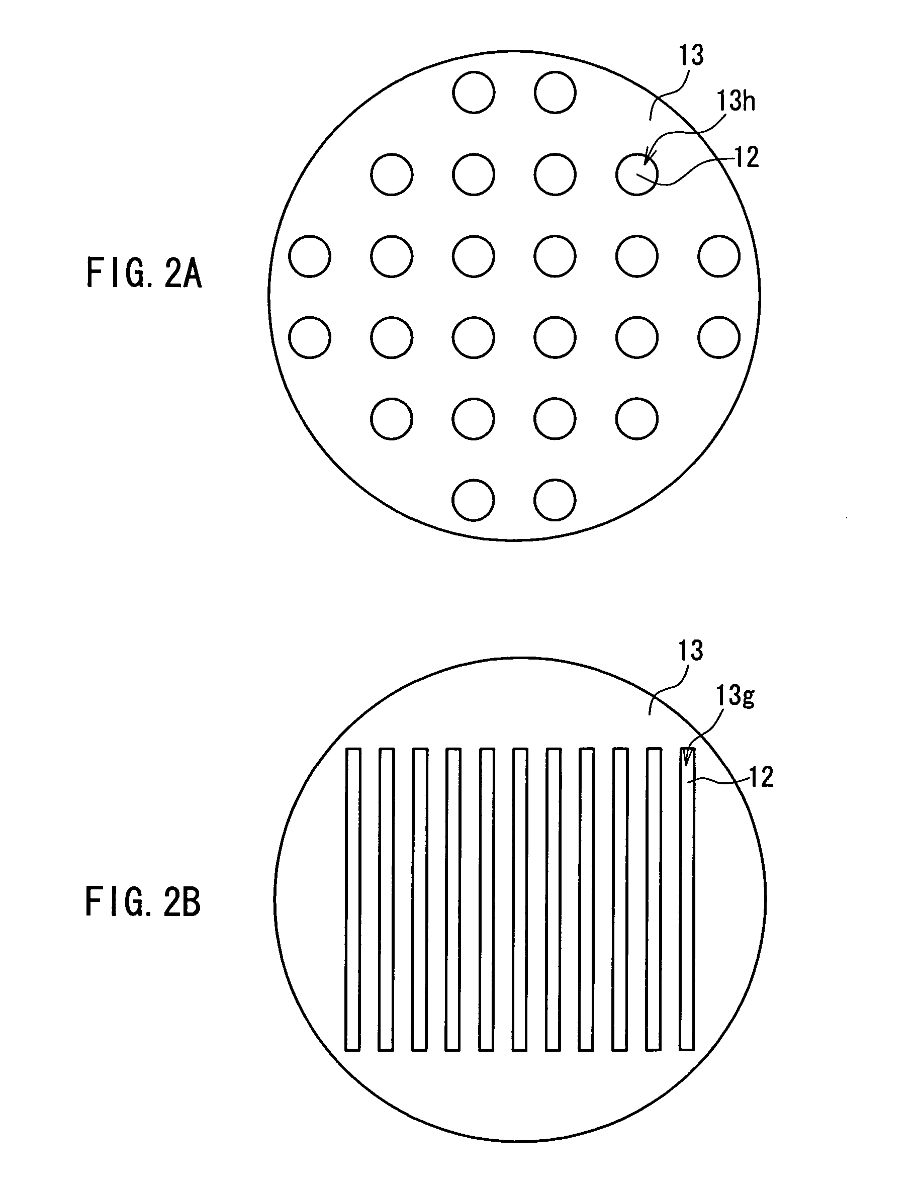
[0075]FIGS. 3A to 3C are cross-sectional views showing an example of steps of the second manufacturing method according to the present invention. As shown in FIG. 3A, a patterned mask film 32 is formed on a base substrate 11 (step (I)). The mask film 32 may be formed of, for instance, silicon nitride, silicon oxide, silicon nitride oxide, aluminum oxide, or aluminum nitride oxide. Furthermore, the mask film may be formed of high melting metal or a high melting metallized material that has a high melting point (a melting point of at least 1000° C.). For instance, titanium, tungsten, molybdenum, niobium, tungsten silicide, molybdenum silicide, or niobium silicide can be used for the mask. The thickness of the mask film 32 is, for example, 0.005 μm to 1 μm, preferably 0.05 μm to 0.5 μm. The method of forming the...
embodiment 3
[0081]The following description is directed to the third manufacturing method of the present invention for manufacturing a Group III nitride substrate.
[0082]In the manufacturing method of Embodiment 3, first, a semiconductor layer that is expressed by a composition formula of AluGavIn1−u−vN (where 0≦u≦1, 0≦v≦1, and u+v≦1) is prepared (step (A)). This step is the same as the step (i) described in Embodiment 1. On this step, the semiconductor layer is, for instance, formed on a base substrate.
[0083]Next, oxidized regions are formed through oxidation of portions of the surface of the semiconductor layer formed in the step (A) (step (B)). The formation of the oxidized regions can prevent crystals from growing from the oxidized portions. The step (B) can be carried out by, for instance, steps (B-1) to (B-3) described below.
[0084]First, a patterned mask film is formed on the surface of the semiconductor layer (step (B-1)). The mask film can be patterned and formed using known materials an...
PUM
 Abstract
Description
Claims
Application Information