Imaging system

a technology of a system and a blinker, applied in the field of imaging systems, can solve the problems of noise signal, difficult to achieve the demand particularly concerning high sensitivity and high-speed reading, and insufficient semiconductor performance of amorphous silicon, and achieve the effects of extracting and removing blinker noise, simple processing, and simple processing

Active Publication Date: 2016-10-18
CANON KK
View PDF23 Cites 35 Cited by
  • Summary
  • Abstract
  • Description
  • Claims
  • Application Information

AI Technical Summary

Benefits of technology

[0008]The present invention has an object to provide an imaging system capable of extracting and removing blinker noise with simple processing without a special mechanism. The imaging system according to one embodiment of the present invention includes: a conversion unit configured to convert radiation into light; a plurality of pixels each configured to convert the light converted by the conversion unit into an electrical signal; an extracting unit configured to extract, based on an image formed based on output signals output from the plurality of pixels, a pixel in which noise is generated due to the radiation that has transmitted through the conversion unit to arrive at the plurality of pixels; and a correcting unit configured to perform correction to remove the noise with respect to an output signal output from the pixel extracted by the extracting unit, in which the extracting unit is configured to extract the pixel in which the noise is generated by performing division between a first image and a second image, the first image being formed based on the output signals output from the plurality of pixels in accordance with the radiation exposed to the conversion unit during a first period in a radiation exposure period during which the radiation is exposed to the conversion unit, the second image being formed based on the output signals output from the plurality of pixels in accordance with the radiation exposed to the conversion unit during a second period provided after the first period in the radiation exposure period. The imaging system can extract and remove the blinker noise with simple processing, and the diagnosis performance can be enhanced. Further, the noise can be removed without requiring a special mechanism or member, and hence increase in cost can be suppressed.

Problems solved by technology

However, amorphous silicon has insufficient semiconductor performance, which makes it difficult to achieve the demand particularly concerning high sensitivity and high-speed reading.
In this case, there arises a problem in that a noise signal caused by direct incident radiation is superimposed on an image signal generated by the visible light.
However, in the method of Japanese Patent No. 3894534, unless exactly the same amount of radiation is exposed when reading the first signal and the second signal that are read twice in the radiation exposure time period, when the difference between the first signal and the second signal is calculated, the object component cannot be completely removed, which causes failure in extraction of the blinker noise component.
Therefore, it is virtually impossible to control the amount of radiation exposed when reading the first signal and the amount of radiation exposed when reading the second signal to be exactly the same.

Method used


Image

  • Imaging system
  • Imaging system
  • Imaging system

Examples


first embodiment

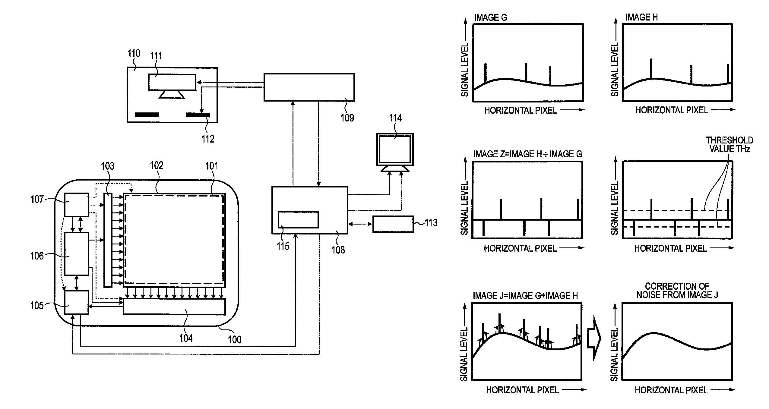
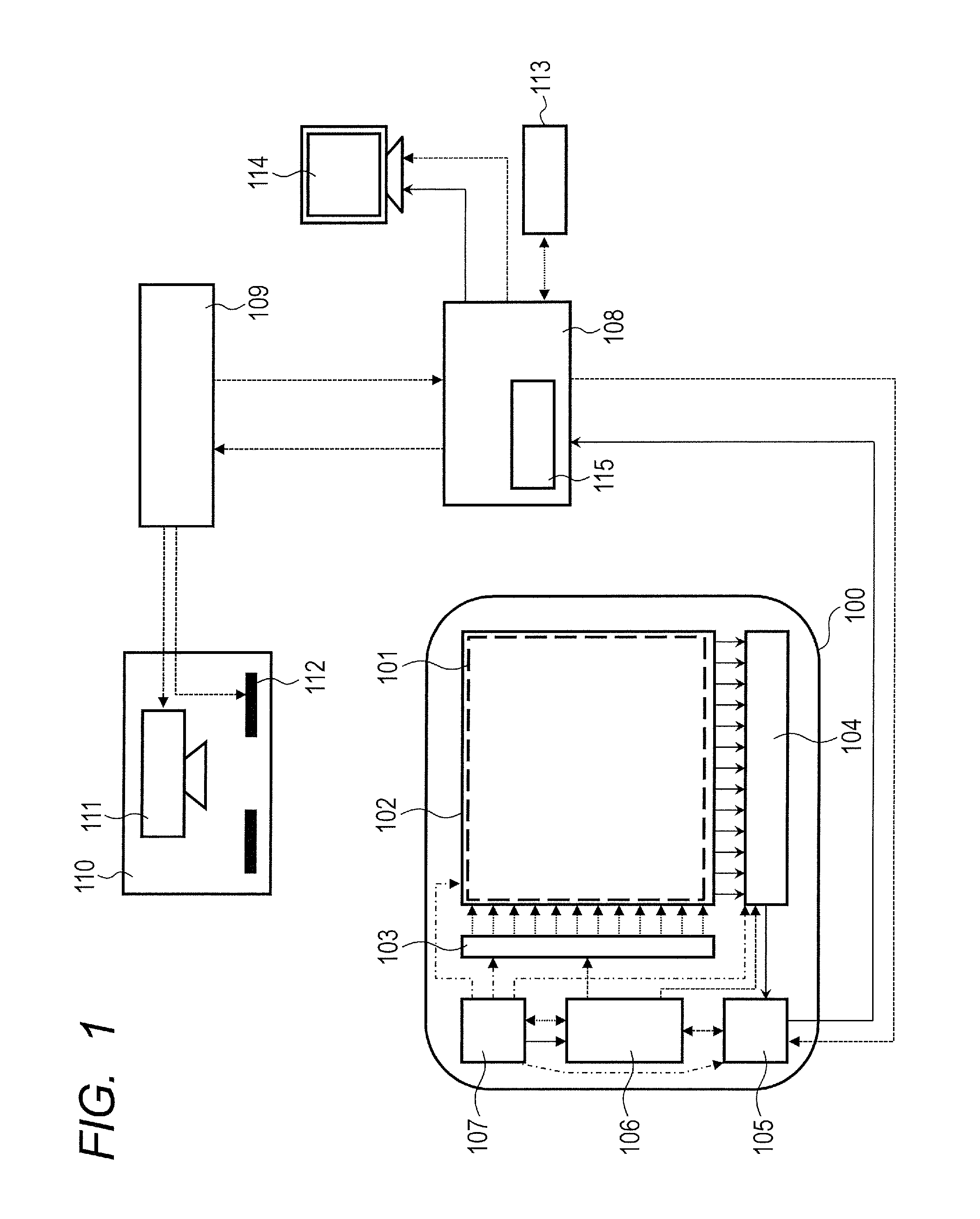
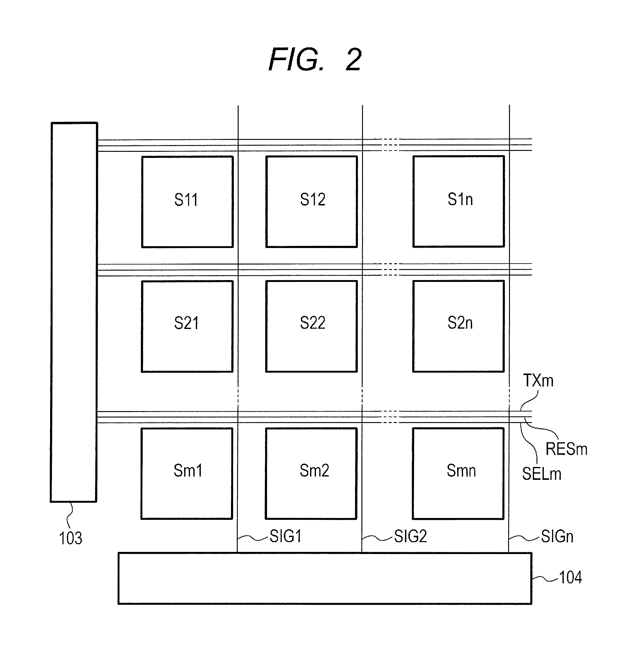
[0022]FIG. 1 is a diagram illustrating a configuration example of a radiation imaging system according to a first embodiment of the present invention. The radiation imaging system includes an imaging apparatus 100, a computer 108, a radiation control apparatus 109, a radiation generating apparatus 110, a console 113, and a display apparatus 114. The radiation generating apparatus 110 emits radiation (for example, X-rays). The imaging apparatus 100 includes a scintillator 101, an imaging element 102, a driver circuit 103, a reading circuit 104, a signal processing section 105, a control section 106, and a power supply section 107. The scintillator 101 is a conversion unit configured to convert radiation into light with a wavelength band that is detectable by the imaging element (photoelectric conversion element) 102. The imaging element 102 includes a plurality of pixels each configured to convert light converted by the scintillator 101 into an electrical signal. The driver circuit 1...

second embodiment

[0049]An imaging apparatus according to a second embodiment of the present invention has a configuration similar to that in the first embodiment illustrated in FIGS. 1, 2, and 3, and hence detailed description thereof is omitted herein. This embodiment differs from the first embodiment in that the reading operation is performed twice or more during the radiation exposure and once or more after the exposure. Thus, this embodiment refers to a processing method when three or more images are acquired.

[0050]FIG. 8 simply illustrates the reading operation when the image is read three times in a single radiation exposure. In FIG. 8, the radiation exposure period is set to t1+t2+t3, and through first reading during the radiation exposure, an image of charges generated through the radiation exposure during the period t1 is read as an image D. Next, through second reading during the radiation exposure, an image of charges generated through the radiation exposure during the period t1+t2 is rea...

third embodiment

[0056]In a third embodiment of the present invention, a method of performing reading by a method that does not leave an electrical signal inside the pixel after the reading processing, and an arithmetic processing method of a case where the reading is performed by this method are described with reference to FIGS. 10, 11, and 12. In the first embodiment (FIGS. 4 and 5), the reset transistor M1 does not reset the plurality of pixels S11 to Smn in a period after the first image A is output in accordance with the radiation during the first period t1 and before the second image b is output in accordance with the radiation during the second period t2. Further, in the second embodiment (FIG. 8), the reset transistor M1 does not reset the plurality of pixels S11 to Smn in a period after the first image D is output in accordance with the radiation during the first period t1 and before the second image F is output in accordance with the radiation during the second period t3. In contrast, in t...


PUM


Abstract

An imaging system comprises: a plurality of pixels each for converting light, converted from radiation by a conversion unit, into an electrical signal; an extracting unit that extracts, based on an image formed based on output signals from the pixels, a pixel with noise generated by the radiation that has transmitted through the conversion unit to arrive at the pixels; and a correcting unit that performs correction to remove the noise with respect to an output signal from the extracted pixel, wherein the extracting unit extracts the pixel with the noise by performing division between first and second images, the first image being formed based on the output signals from the pixels in accordance with the radiation to the conversion unit during a first period, the second image being formed based on these output signals in accordance with that radiation during a second period after the first period.

Description

BACKGROUND OF THE INVENTION[0001]1. Field of the Invention[0002]The present invention relates to an imaging system that is suitably used in a medical diagnosis to take a still image, such as in general radiography, or to take a moving image, such as in fluoroscopy.[0003]2. Description of the Related Art[0004]In recent years, a radiation imaging apparatus using a flat panel detector (hereinafter simply referred to as “detector”) that is made of a semiconductor material has come into practical use as an imaging apparatus used in a medical image diagnosis or a nondestructive inspection by radiation. For example, in the medical image diagnosis, such radiation imaging apparatus is used as a digital imaging apparatus to take a still image, such as in general radiography, or to take a moving image, such as in fluoroscopy. As the detector, there is known an indirect-conversion detector obtained by combining a scintillator configured to convert radiation into light with a wavelength band tha...

Claims


Application Information

Patent Timeline
Patent Type & Authority Patents(United States)
IPC IPC(8): A61B6/00G01T7/00H04N5/32H04N5/357G06T5/00G06T5/50H04N5/325H04N5/347G01T1/20H04N5/378H04N5/217
CPCA61B6/5258A61B6/5205G06T5/002G06T5/50H04N5/357A61B6/42A61B6/52A61B6/585G01T1/2018G01T7/005H04N5/2173H04N5/32H04N5/325H04N5/3205H04N5/347H04N5/378H04N25/60G01T1/20184H04N25/46H04N25/75
Inventor RYU, TAKUYAKAMESHIMA, TOSHIOYAGI, TOMOYUKITAKENAKA, KATSUROSATO, SHOIWASHITA, ATSUSHISATO, ERIKOOKADA, HIDEYUKI
Owner CANON KK
Why Eureka
Try Eureka