SiC transient voltage suppressor
a transient voltage and suppressor technology, applied in the direction of basic electric elements, electrical equipment, semiconductor devices, etc., can solve problems such as devices being destroyed
- Summary
- Abstract
- Description
- Claims
- Application Information
AI Technical Summary
Benefits of technology
Problems solved by technology
Method used
Image
Examples
first embodiment
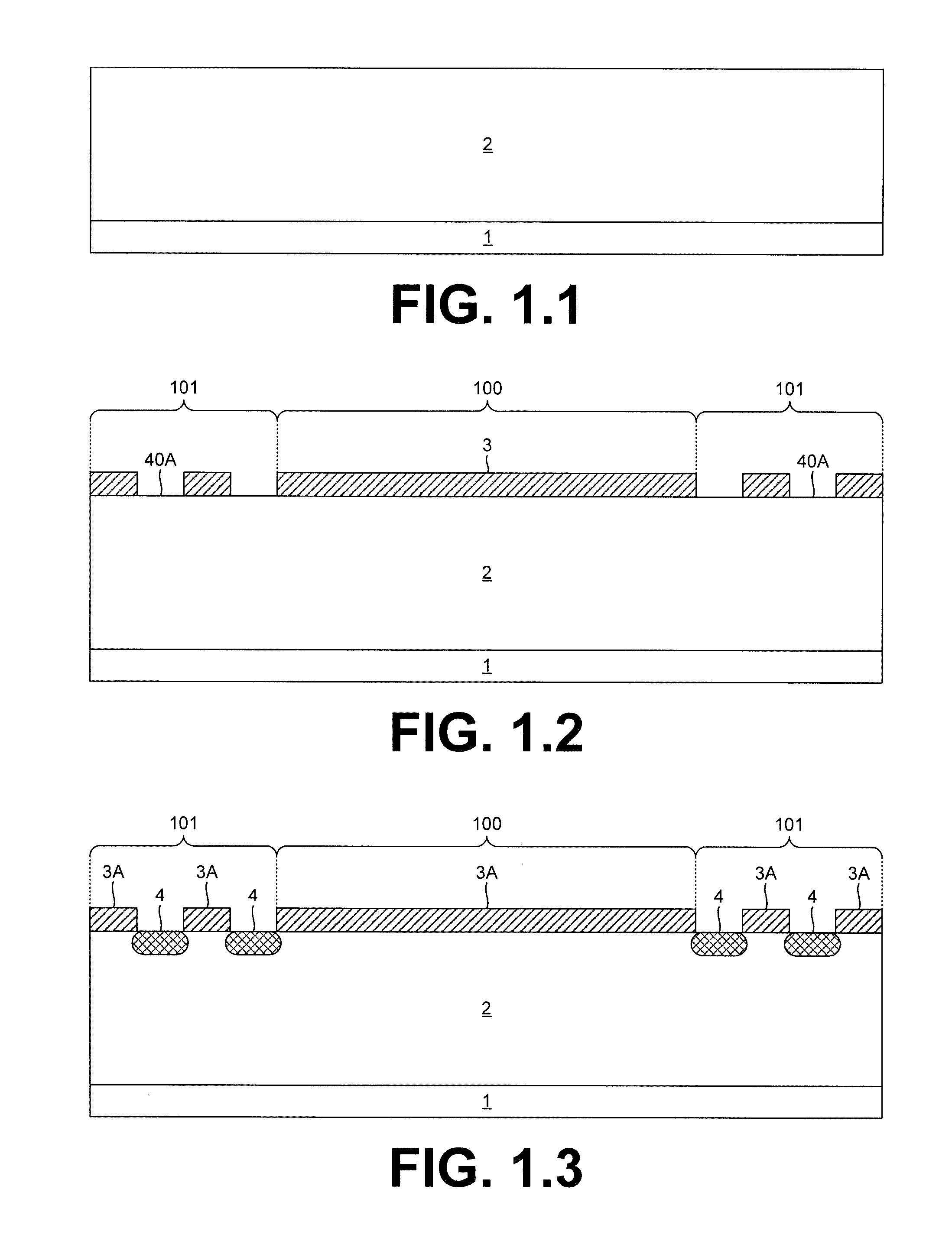
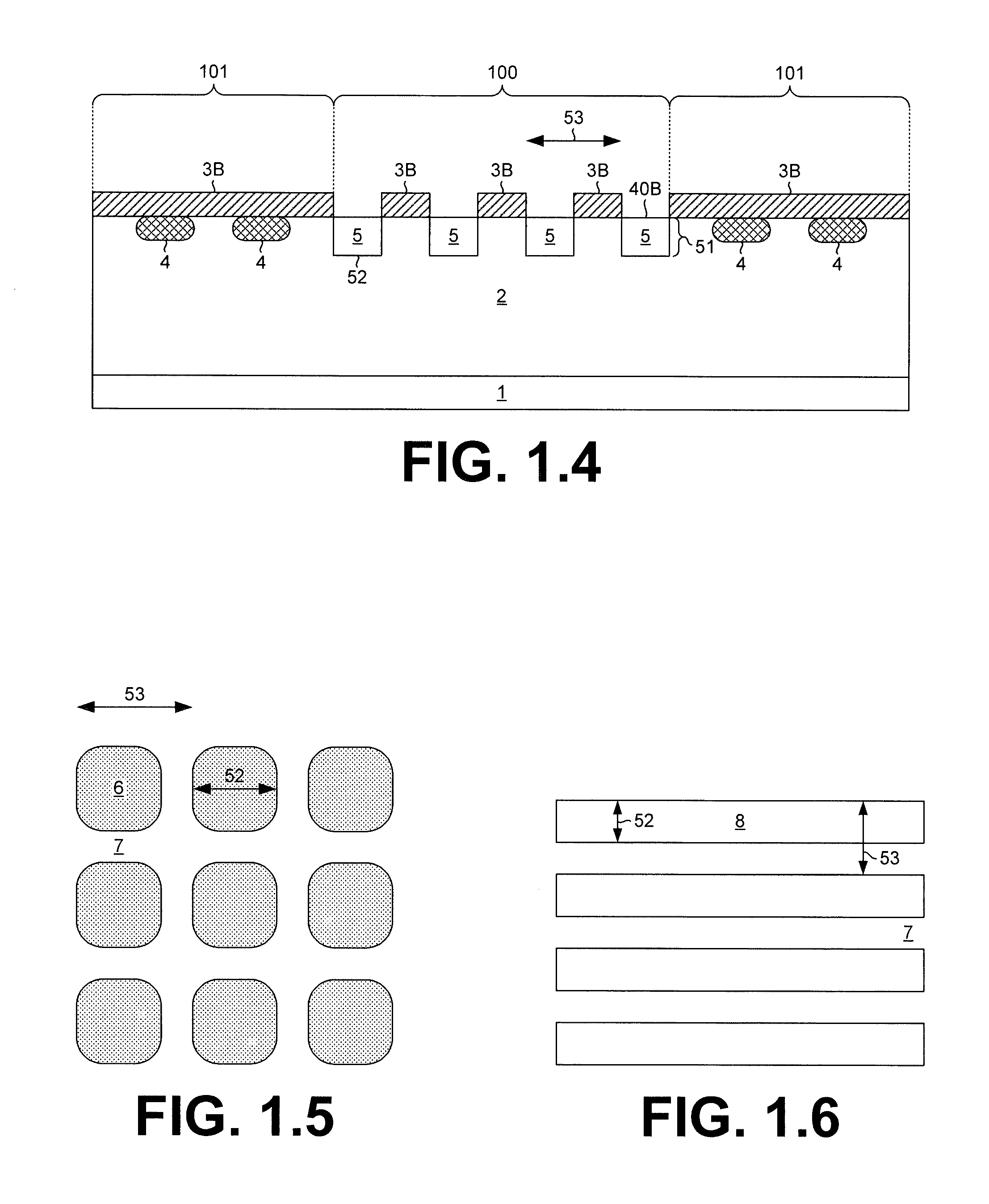
[0032]In the first embodiment, as seen in FIG. 1.9 or 1.10, a higher voltage TVS is targeted (e.g., targeted voltage 500-800V). In this case, the active area avalanche is forced to take place by the depth and the placement (layout design) of the trenches 5 in the SiC material. The top part of the structure and the bottom of the trenches are implanted with Aluminum, forming a P-type doping 9, and therefore a P-N junction. In some embodiments, such as FIG. 1.10, the sides of the trenches are set with proper Schottky barrier metals to create a Schottky barrier diode 50 on the side walls of the trenches, and in this way the forward voltage of the TVS is even lower, a very advantageous feature of the final device.
[0033]The depth and the placement of the trenches create high electric fields at the bottom (and the corners) of the trenches, and therefore the first avalanche of the TVS will take place at those locations. Since the breakdown voltage has a positive temperature coefficient, the...
second embodiment
[0053]In a second embodiment, as seen in FIG. 2.4, a mid-range voltage TVS is enabled (100-500V range). In order to induce an active area avalanche, a heavier doping of the epitaxial layer is employed towards the anode region. The heavier doping at the top surface of the wafers can be easily achieved during the epitaxial process where a first epitaxial layer 2 (grown right on the top of the substrate) has a doping in the example range of 1E15 to 8E15 atoms / cm3 while a top epitaxial layer 21 (grown sequentially after the growth of the first layer was completed) can have a doping in the example range of 2E16 to 1E17 atoms / cm3. The targeted breakdown voltage is 30-100V which is tailored by the doping of the top epitaxial layer 21. TCAD simulations or analytical or experimental data can provide the data required to make the design of the doping of the second epitaxial layer for the desired BV of the product. A high voltage termination in the form of floating P-rings 24B are formed in a ...
PUM
 Abstract
Description
Claims
Application Information


