Sic transient voltage suppressor

a transient voltage and suppressor technology, applied in the direction of basic electric elements, electrical equipment, semiconductor devices, etc., can solve problems such as devices being destroyed

Active Publication Date: 2016-05-05
MICROSEMI
View PDF1 Cites 11 Cited by
  • Summary
  • Abstract
  • Description
  • Claims
  • Application Information

AI Technical Summary

Benefits of technology

[0010]For space applications, a radiation-hardened TVS is mandatory to be used. During heavy ion bombardment a high charge is created and under high electric field that charge can easily multiply and the power conditions (and therefore t

Problems solved by technology

During heavy ion bombardment a high charge is created and under high electric field that charge can easily

Method used


Image

  • Sic transient voltage suppressor
  • Sic transient voltage suppressor
  • Sic transient voltage suppressor

Examples


first embodiment

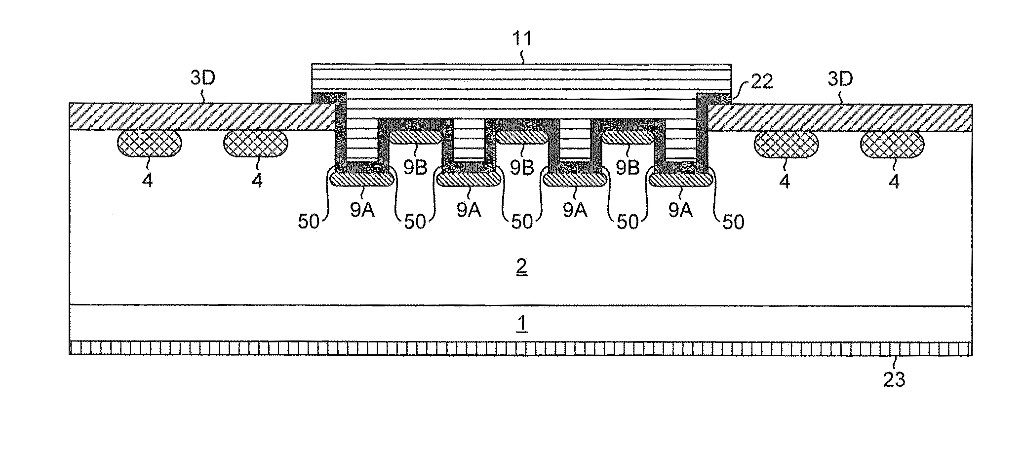
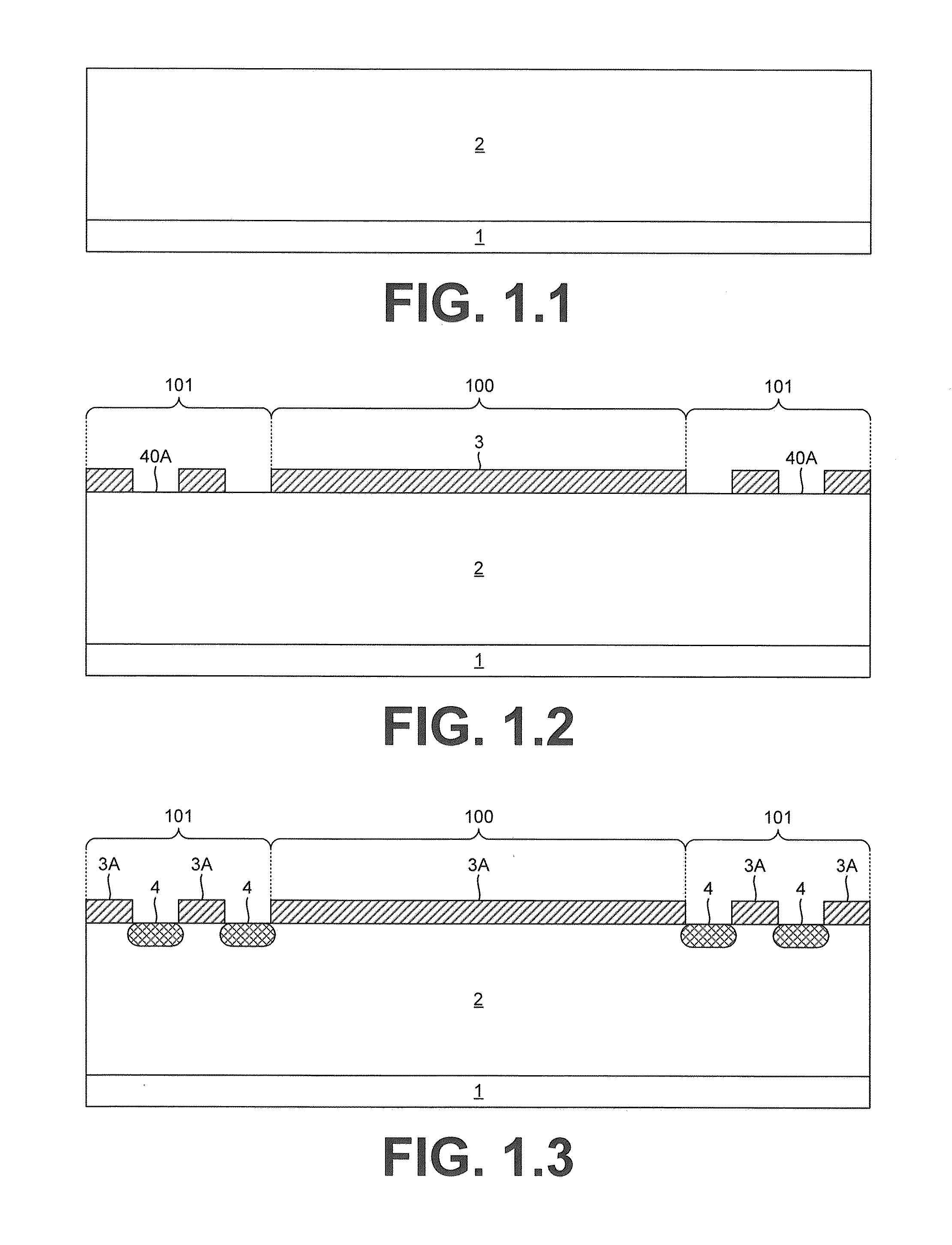
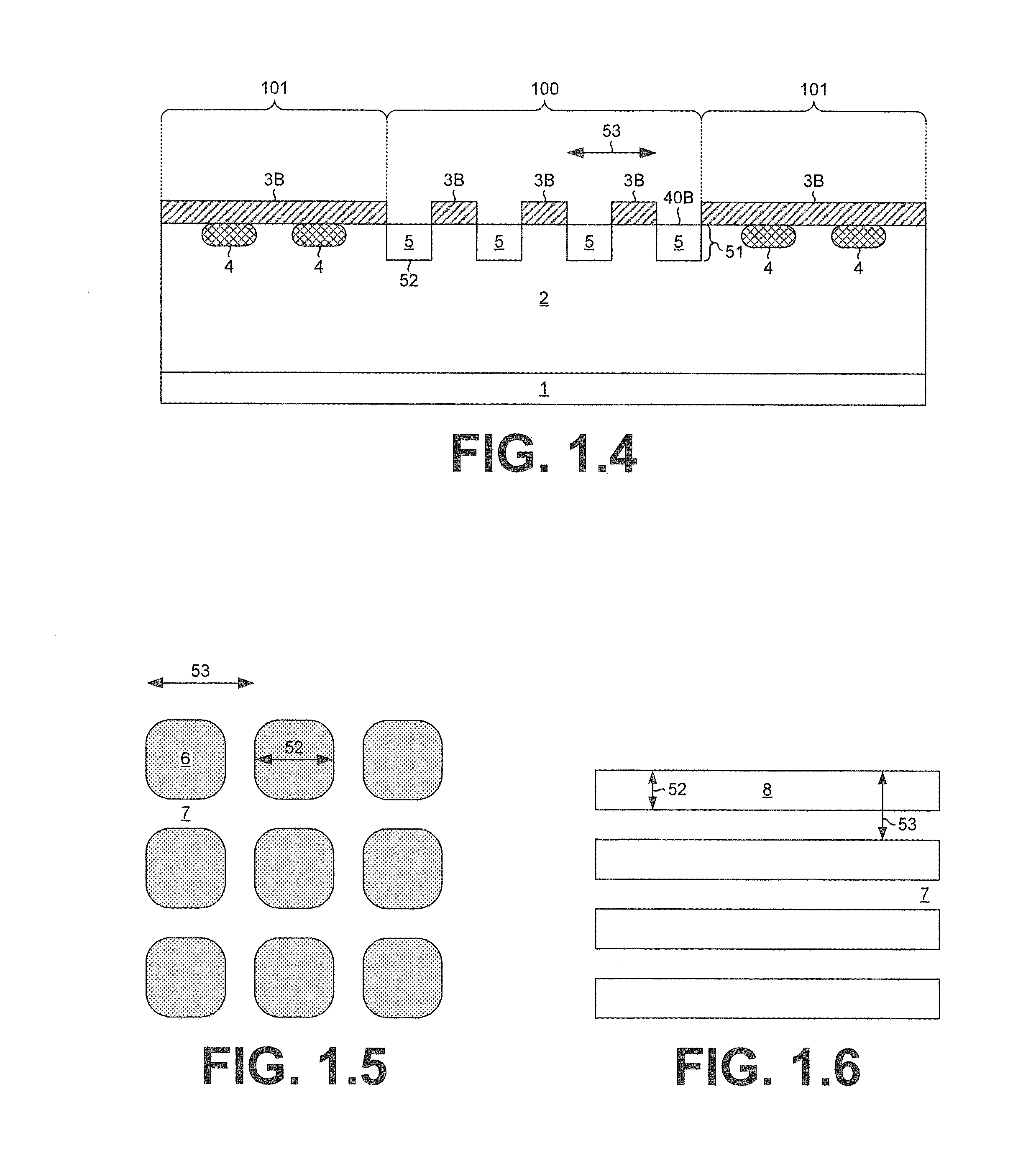
[0032]In the first embodiment, as seen in FIG. 1.9 or 1.10, a higher voltage TVS is targeted (e.g., targeted voltage 500-800V). In this case, the active area avalanche is forced to take place by the depth and the placement (layout design) of the trenches 5 in the SiC material. The top part of the structure and the bottom of the trenches are implanted with Aluminum, forming a P-type doping 9, and therefore a P-N junction. In some embodiments, such as FIG. 1.10, the sides of the trenches are set with proper Schottky barrier metals to create a Schottky barrier diode 50 on the side walls of the trenches, and in this way the forward voltage of the TVS is even lower, a very advantageous feature of the final device.

[0033]The depth and the placement of the trenches create high electric fields at the bottom (and the corners) of the trenches, and therefore the first avalanche of the TVS will take place at those locations. Since the breakdown voltage has a positive temperature coefficient, the...

second embodiment

[0053]In a second embodiment, as seen in FIG. 2.4, a mid-range voltage TVS is enabled (100-500V range). In order to induce an active area avalanche, a heavier doping of the epitaxial layer is employed towards the anode region. The heavier doping at the top surface of the wafers can be easily achieved during the epitaxial process where a first epitaxial layer 2 (grown right on the top of the substrate) has a doping in the example range of 1E15 to 8E15 atoms / cm3 while a top epitaxial layer 21 (grown sequentially after the growth of the first layer was completed) can have a doping in the example range of 2E16 to 1E17 atoms / cm3. The targeted breakdown voltage is 30-100V which is tailored by the doping of the top epitaxial layer 21. TCAD simulations or analytical or experimental data can provide the data required to make the design of the doping of the second epitaxial layer for the desired BV of the product. A high voltage termination in the form of floating P-rings 24B are formed in a ...


PUM


Abstract

A high power, high current Unidirectional Transient Voltage Suppressor, formed on SiC starting material is disclosed. The device is structured to avalanche uniformly across the entire central part (active area) such that very high currents can flow while the device is reversely biased. Forcing the device to avalanche uniformly across designated areas is achieved in different ways but consistently in concept, by creating high electric fields where the device is supposed to avalanche (namely the to active area) and by relaxing the electric field across the edge of the structure (namely in the termination), which in all embodiments meets the conditions for an increased reliability under harsh environments.

Description

CROSS REFERENCE TO RELATED APPLICATION[0001]This application claims the benefit of copending U.S. provisional patent application 61 / 939,286, filed Feb. 13, 2014, incorporated by reference herein.BACKGROUND OF THE INVENTION[0002]The main circuit function performed by a Transient Voltage Suppressor (TVS) is to protect the active elements of the circuit from unexpected transient voltage spikes. These sudden and unexpected transient voltage spikes can be generated by natural causes (lightning being the most common one) or by other high power equipments, operating in close proximity to the sensitive electronic circuit.[0003]The TVS function can be achieved with various devices, most common ones being Metal Oxide Varistors (MOVs), Zener or P-N Junctions operating in avalanche (Semiconductor Avalanche Diodes, or SADs) and by Crowbar Elements (like Gas Discharge).[0004]TVS devices can be made to block (clamp) voltage in one direction (one polarity of the applied voltage) and in this case th...

Claims


Application Information

Patent Timeline
IPC IPC(8): H01L29/06H01L29/16H01L29/36H01L29/872
CPCH01L29/0626H01L29/872H01L29/0619H01L29/36H01L29/1608H01L29/402H01L29/6606H01L27/0248H01L29/861H01L29/6603H01L29/8618
Inventor SDRULLA, DUMITRUODEKIRK, BRUCEWALTERS, CECIL KENT
Owner MICROSEMI
Why Eureka
Try Eureka