
Flippable leadframe for packaged electronic system having vertically stacked chips and components

a technology of leadframes and electronic systems, applied in the direction of semiconductor devices, semiconductor/solid-state device details, electrical apparatus, etc., can solve the problems of difficult alignment, difficult to control coplanarity, and excessive manual handling, and achieve the effect of difficult alignmen

Active Publication Date: 2016-11-15
TEXAS INSTR INC
View PDF7 Cites 1 Cited by
  • Summary
  • Abstract
  • Description
  • Claims
  • Application Information

AI Technical Summary

Benefits of technology

This approach simplifies the assembly process, reduces misalignment, and allows for compact packaging with improved reliability by enabling easy alignment and encapsulation of passive components in close proximity to active chips.

Problems solved by technology

Applicants realized that in conventional semiconductor manufacturing, the advantage of using two leadframes on semiconductor devices with needs for high density stacking is frequently offset by the disadvantage of excessive manual handling, difficult alignments, and hard-to-control coplanarity.
Difficulties of achieving compactness and avoiding misalignment and solder reflow limitations are compiled when passive components have to be merged in close proximity to active chips.

Method used


Image

  • Flippable leadframe for packaged electronic system having vertically stacked chips and components
  • Flippable leadframe for packaged electronic system having vertically stacked chips and components
  • Flippable leadframe for packaged electronic system having vertically stacked chips and components

Examples


Embodiment Construction

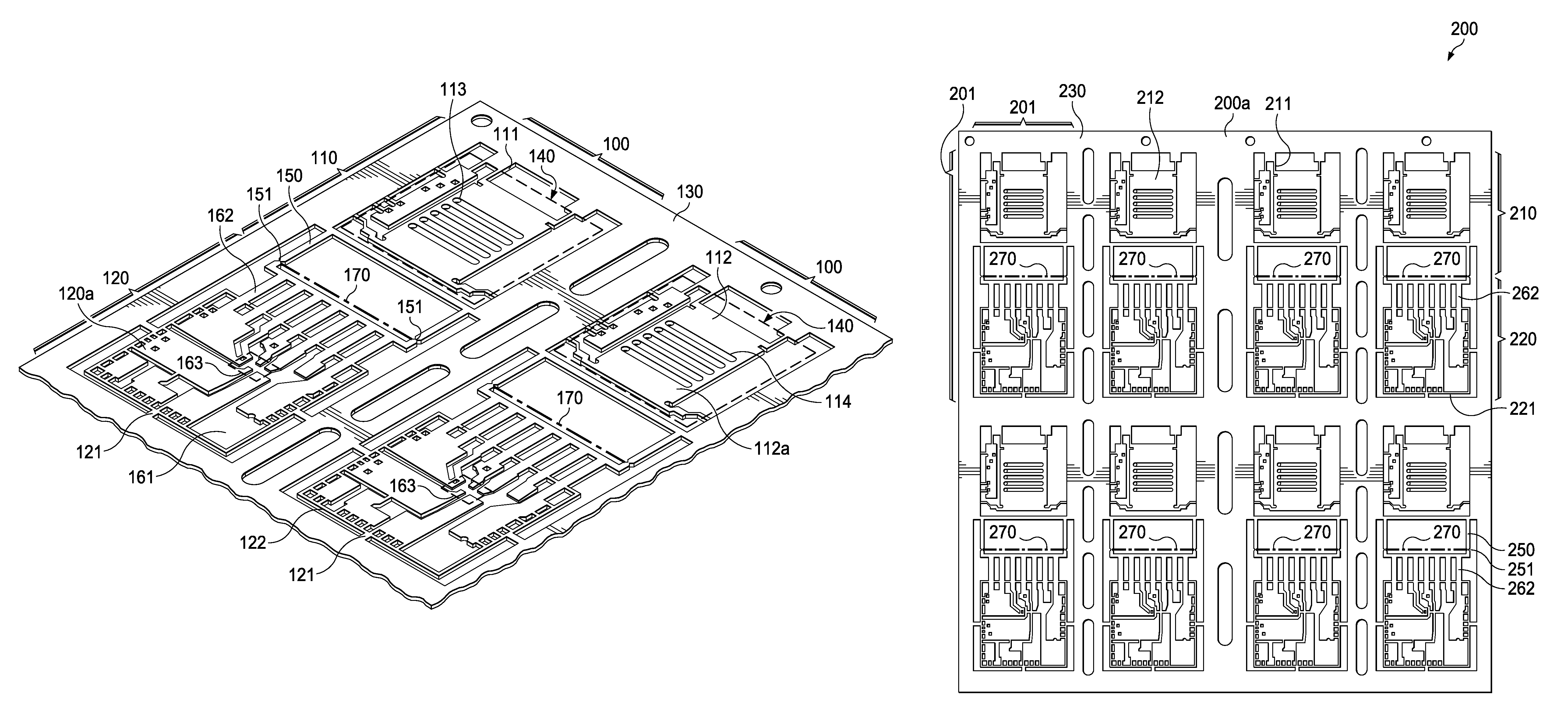
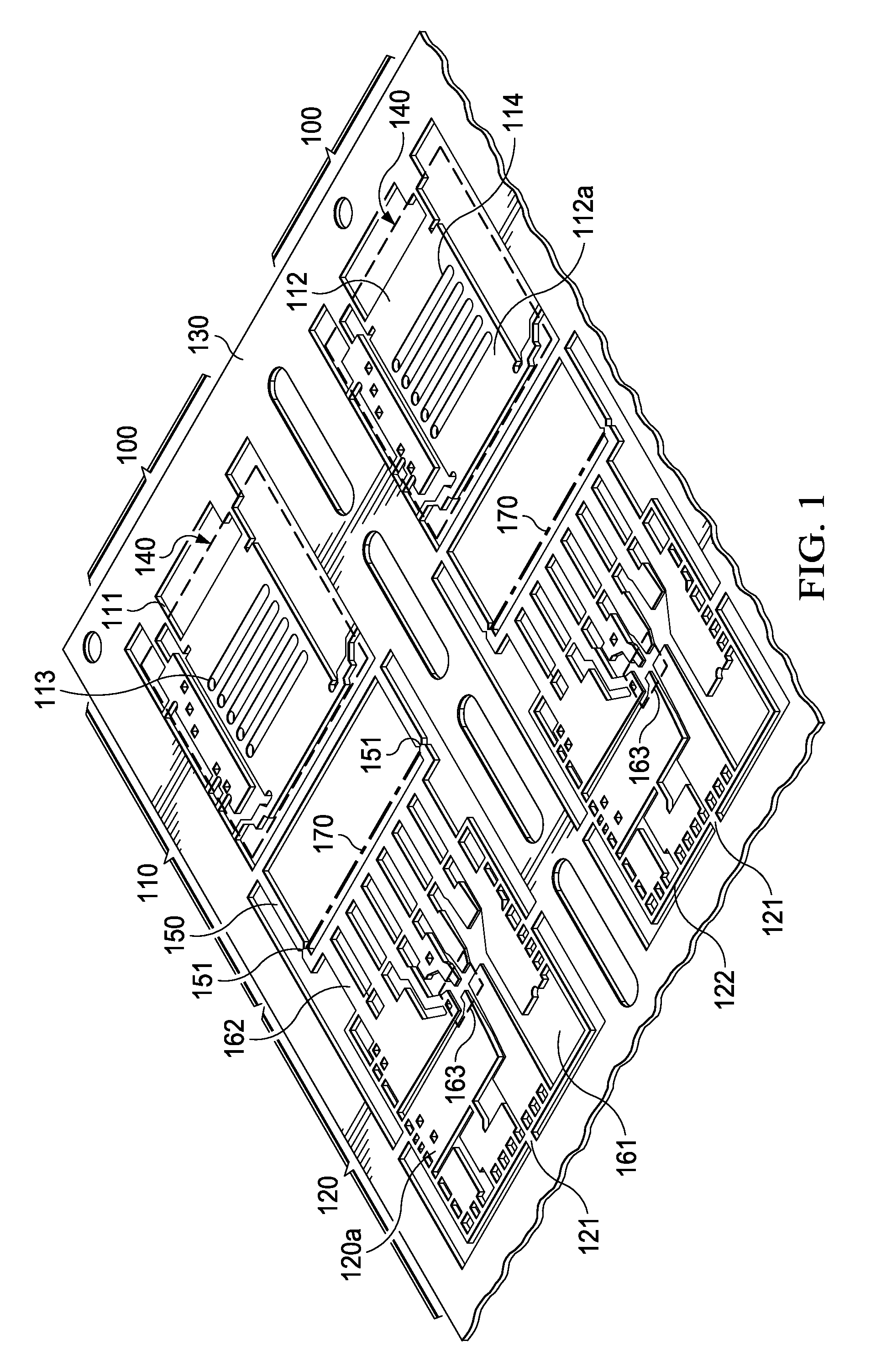
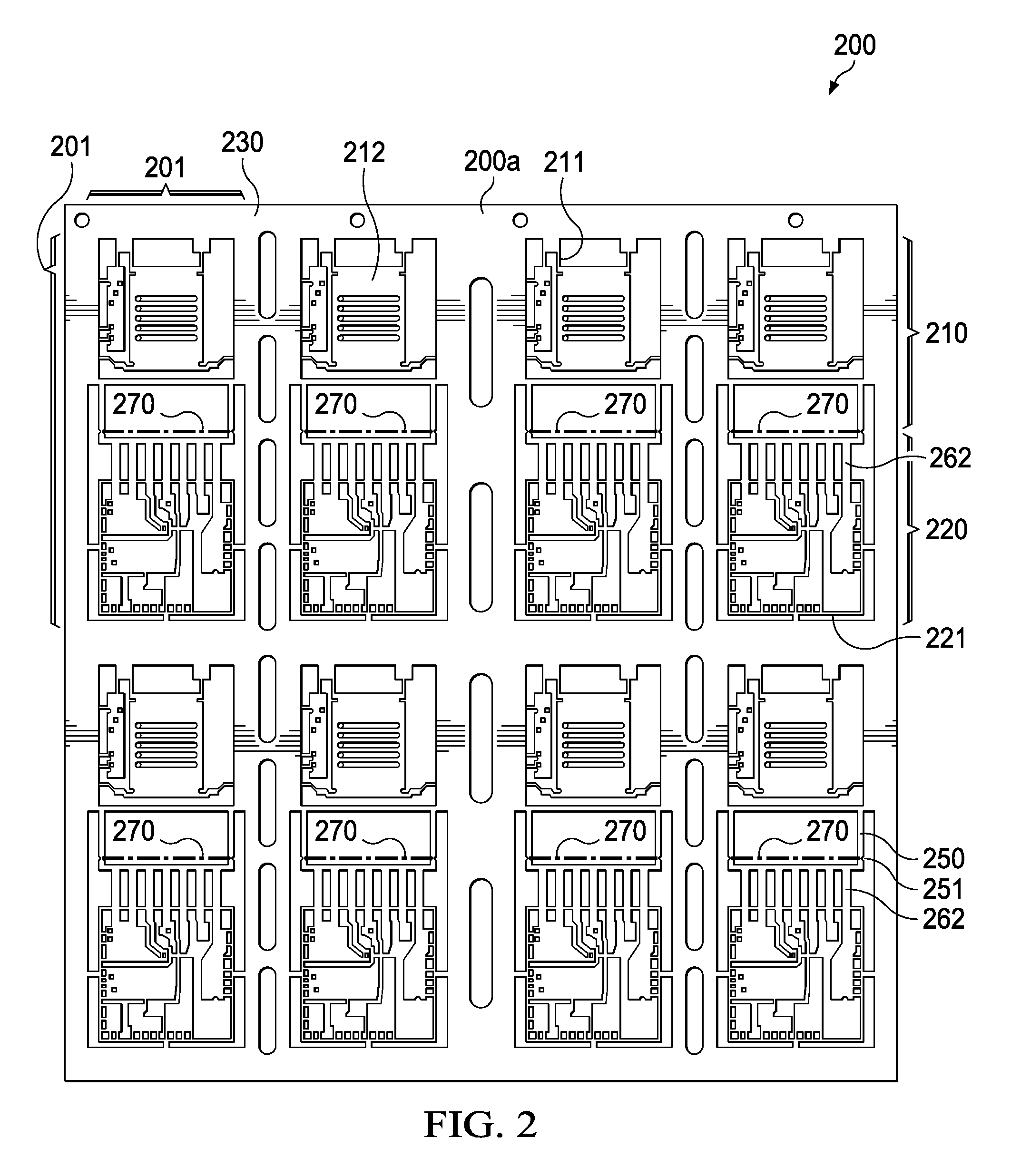
[0019]An exemplary embodiment of the invention is a leadframe as illustrated in FIG. 1 and generally designated 100. For cost-effective manufacturing and enabling batch-processing, it is practical to start with a leadframe strip 200 as shown in FIG. 2, which includes a plurality of leadframes 100. Leadframe strip 200 is stamped or etched from a flat sheet of metal selected from a group including copper, copper alloys, aluminum, iron-nickel alloys, and Kovar™. When the metal sheet is made of copper, the preferred thickness of the sheet is between 100 and 300 μm. For some applications, the sheet may be thicker or thinner. The metal sheet has a first surface and an opposite second surface. In FIGS. 1 and 2, the first surface is depicted and the opposite second surface is nor shown. The metallurgical preparation of the second surface may be the same as the first surface, or it may be different. As an example, one surface, or at least a portion of the surface, may be prepared for facilit...


PUM


Abstract

A leadframe (100) for electronic systems comprising a first sub-leadframe (110) connected by links (150) to a second sub-leadframe (120), the first and second sub-leadframe connected by tiebars (111, 121) to a frame (130); and each link having a neck (151) suitable for bending the link, the necks arrayed in a line (170) operable as the axis for bending the second sub-leadframe towards the first sub-leadframe with the necks operable as rotation pivots.

Description

FIELD[0001]Embodiments of the invention are related in general to the field of semiconductor devices and processes, and more specifically to the structure and fabrication method of packaged electronic systems having a plurality of leadframes, vertically stacked by folding, together with semiconductor chips and passive components.DESCRIPTION OF RELATED ART[0002]Driven by the desire to reduce the board area needed to assemble a semiconductor device into electronic products such as hand-held telephones, today's semiconductor devices often use vertically stacked chips inside the packages. These chip stacks frequently include chips of significantly different sizes, assembled mostly by wire bonding techniques on interposers commonly made of rigid materials such as ceramics or fiber-enforced plastics such as FR-4 and others.[0003]In applications where a whole system is to be encapsulated into a package, it is desirable to add passive components such as capacitors, resistors, and inductors ...

Claims


Application Information

Patent Timeline
Patent Type & Authority Patents(United States)
IPC IPC(8): H01L21/00H01L21/56H01L21/78H01L21/48H01L23/495H01L23/31
CPCH01L23/49555H01L21/4825H01L21/4842H01L21/565H01L21/78H01L23/3114H01L23/49503H01L23/49537H01L23/49568H01L23/49586H01L2224/97H01L23/49589H10K71/00H01L23/49551
Inventor EUGENE LEE, LEE HAN MENG@BIN ABDUL AZIZ, ANIS FAUZIFEN, SUEANN LIM WEI
Owner TEXAS INSTR INC
Learn More