Semiconductor device including oxide semiconductor stack with different ratio of indium and gallium

a technology of indium gallium and semiconductor stack, which is applied in the direction of semiconductor devices, electrical devices, transistors, etc., can solve the problems of change in and achieve the effects of preventing diffusion, reducing energy gap, and stabilizing electrical characteristics of transistors

Active Publication Date: 2016-11-15
SEMICON ENERGY LAB CO LTD
View PDF196 Cites 70 Cited by
  • Summary
  • Abstract
  • Description
  • Claims
  • Application Information

AI Technical Summary

Benefits of technology

[0011]Thus, an object of one embodiment of the present invention is to provide a highly reliable semiconductor device including an oxide semiconductor by preventing a change in its electrical characteristics.
[0024]According to one embodiment of the present invention, a change in the electrical characteristics of a transistor including an oxide semiconductor can be prevented, so that a highly reliable semiconductor device can be provided.

Problems solved by technology

Further, the existence of a trap level at an interface between the oxide semiconductor layer and a gate insulating layer might cause a change in the electrical characteristics of the transistor.

Method used


Image

  • Semiconductor device including oxide semiconductor stack with different ratio of indium and gallium
  • Semiconductor device including oxide semiconductor stack with different ratio of indium and gallium
  • Semiconductor device including oxide semiconductor stack with different ratio of indium and gallium

Examples


embodiment 1

(Embodiment 1)

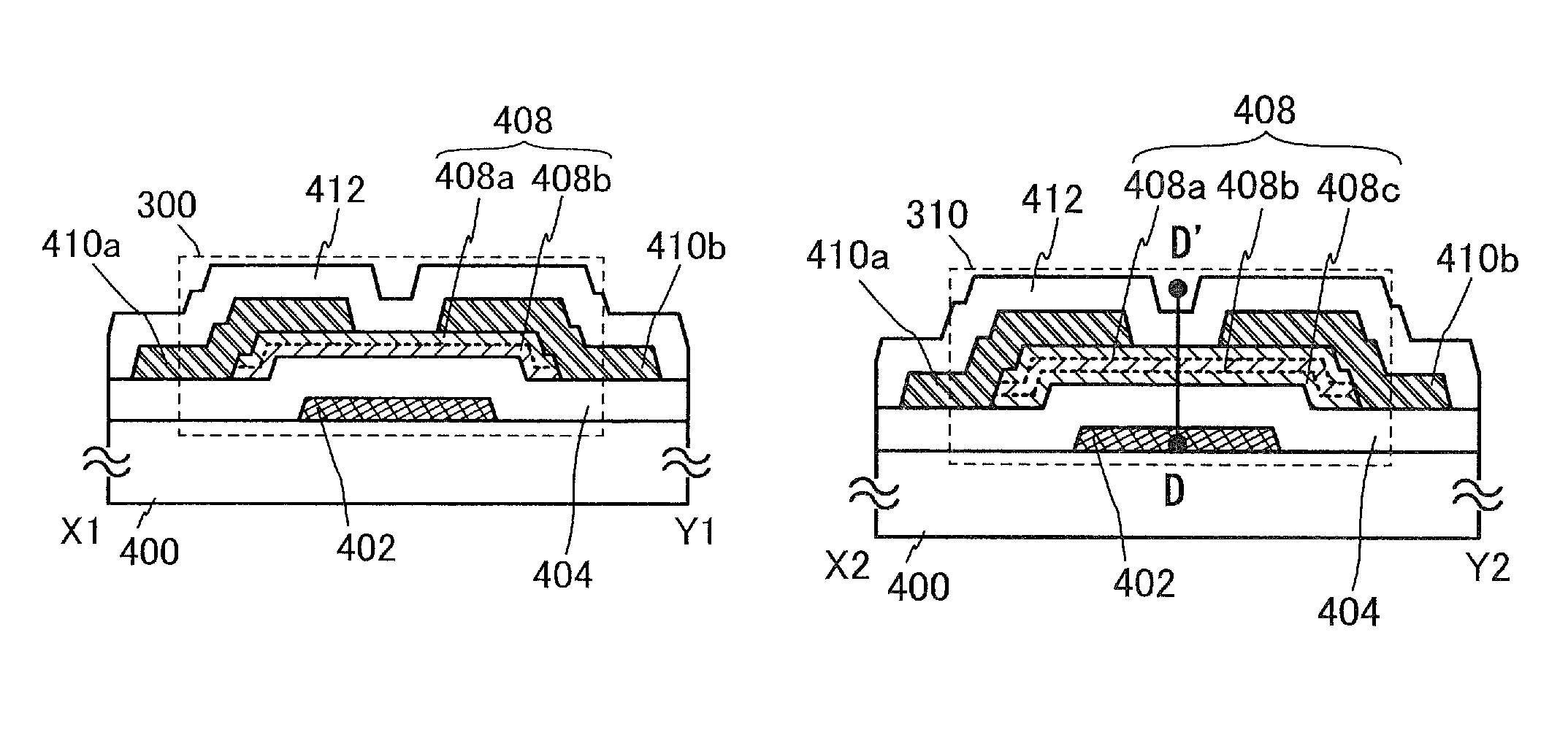
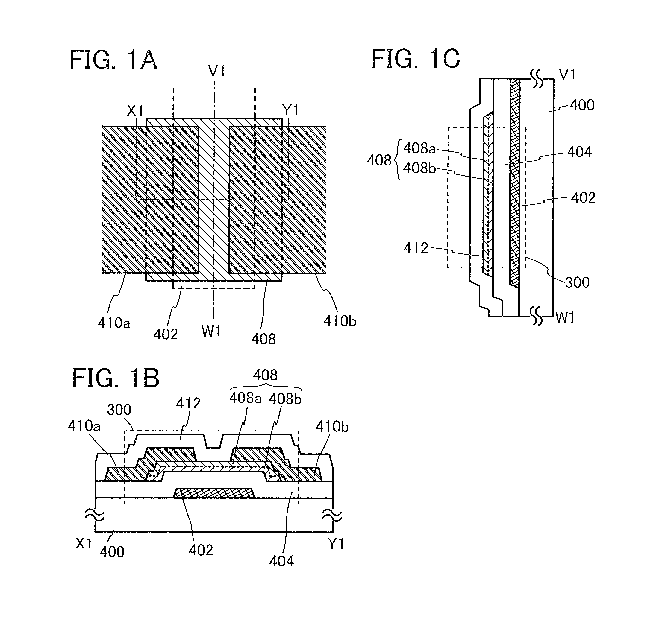
[0044]In this embodiment, one embodiment of a semiconductor device and one embodiment of a method for manufacturing the semiconductor device are described using FIGS. 1A to 1C, FIGS. 2A to 2D, and FIGS. 3A to 3D. In this embodiment, a bottom-gate transistor including an oxide semiconductor layer is described as an example of the semiconductor device.

[0045]FIGS. 1A to 1C illustrate a structure example of a transistor 300. FIG. 1A is a plan view of the transistor 300, FIG. 1B is a cross-sectional view taken along dotted line X1-Y1 in FIG. 1A, and FIG. 1C is a cross-sectional view taken along dotted line V1-W1 in FIG. 1A.

[0046]The transistor 300 includes a gate electrode layer 402 which is provided over a substrate 400 having an insulating surface, a gate insulating layer 404 over the gate electrode layer 402, an oxide semiconductor stack 408 which is on and in contact with the gate insulating layer 404 and overlaps with the gate electrode layer 402, and a source electrod...

embodiment 2

(Embodiment 2)

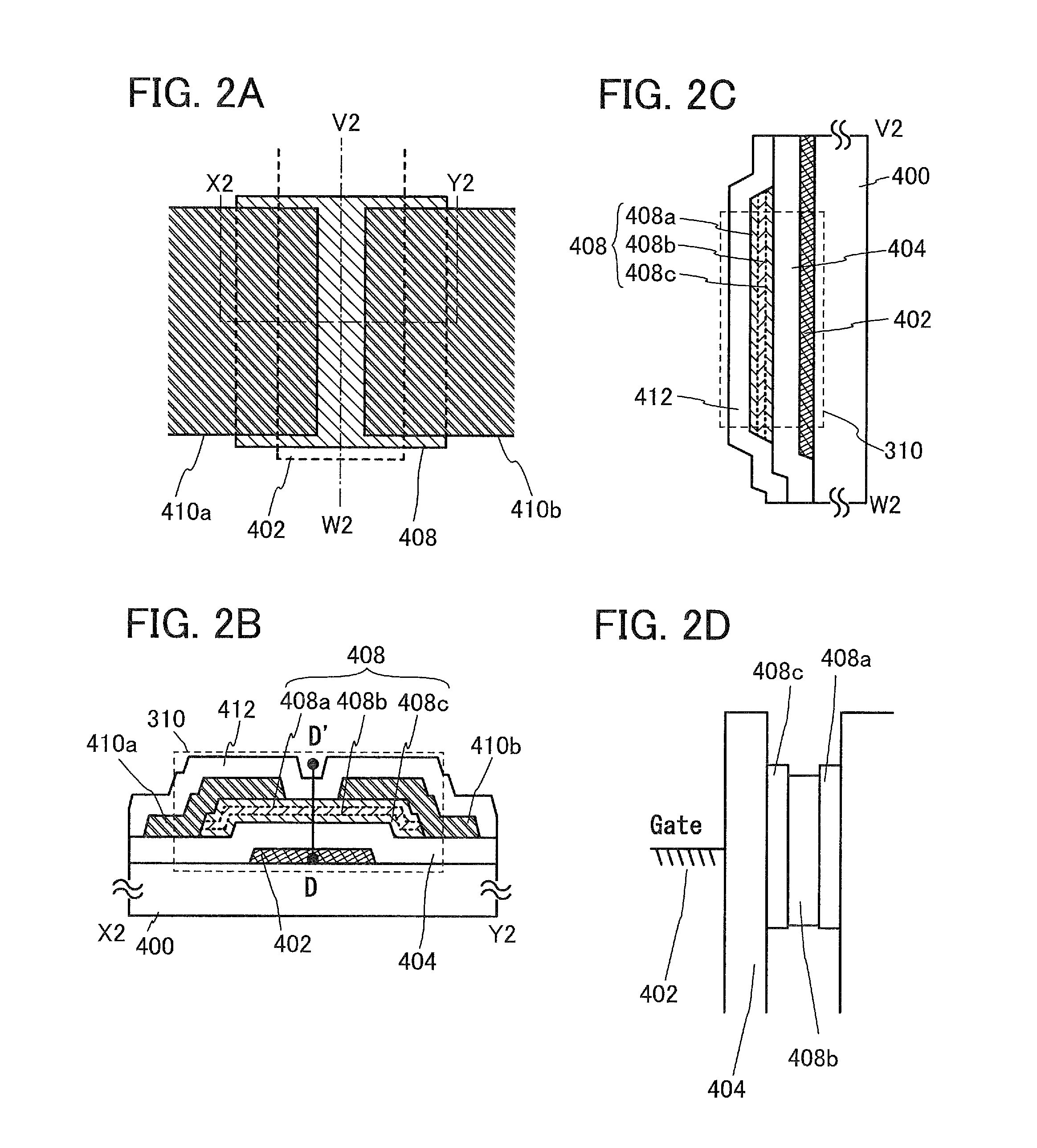
[0134]In this embodiment, an embodiment of a semiconductor device which is different from that in Embodiment 1 will be described with reference to FIGS. 10A and 10B. Specifically, transistors each including a gate insulating layer with a structure which is different from that of the transistor of Embodiment 1 are described.

[0135]A structural example of a transistor 320 is illustrated in FIG. 10A. In a manner similar to the transistor 310 in FIGS. 2A to 2D, the transistor 320 in FIG. 10A includes the gate electrode layer 402 provided over the substrate 400 having an insulating surface, the gate insulating layer 403 and 406 over the gate electrode layer 402, the oxide semiconductor stack 408 which is in contact with the gate insulating layer 406 and overlaps with the gate electrode layer 402, and the source electrode layer 410a and the drain electrode layer 410b which are electrically connected to the oxide semiconductor stack 408. In the transistor 320, the oxide semico...

embodiment 3

(Embodiment 3)

[0152]A semiconductor device having a display function (also referred to as a display device) can be manufactured using the transistor described in Embodiment 1 or 2. Further, part or all of the driver circuitry which includes the transistor can be formed over a substrate where a pixel portion is formed, whereby a system-on-panel can be formed.

[0153]In FIG. 4A, a sealant 4005 is provided so as to surround a pixel portion 4002 provided over a substrate 4001, and the pixel portion 4002 is sealed with a substrate 4006. In FIG. 4A, a scan line driver circuit 4004 and a signal line driver circuit 4003 which are each formed using a single crystal semiconductor film or a polycrystalline semiconductor film over an IC chip or a substrate separately prepared are mounted on the substrate 4001, in a region that is different from the region surrounded by the sealant 4005. Various signals and potentials which are provided to the pixel portion 4002 through the signal line driver circ...


PUM


Abstract

A highly reliable semiconductor device including an oxide semiconductor is provided by preventing a change in its electrical characteristics. A semiconductor device which includes a first oxide semiconductor layer which is in contact with a source electrode layer and a drain electrode layer and a second oxide semiconductor layer which serves as a main current path (channel) of a transistor is provided. The first oxide semiconductor layer serves as a buffer layer for preventing a constituent element of the source and drain electrode layers from diffusing into the channel. By providing the first oxide semiconductor layer, it is possible to prevent diffusion of the constituent element into an interface between the first oxide semiconductor layer and the second oxide semiconductor layer and into the second oxide semiconductor layer.

Description

TECHNICAL FIELD[0001]The invention disclosed in this specification and the like relates to a semiconductor device and a method for manufacturing the semiconductor device.[0002]In this specification and the like, a semiconductor device refers to all types of devices which can function by utilizing semiconductor characteristics; an electro-optical device, an image display device, a semiconductor circuit, and an electronic appliance are all semiconductor devices.BACKGROUND ART[0003]A technique by which transistors are formed using semiconductor thin films formed over a substrate having an insulating surface has been attracting attention. Such a transistor is applied to a wide range of electronic devices such as an integrated circuit (IC) and an image display device (also simply referred to as a display device). A silicon-based semiconductor material is widely known as a material for a semiconductor thin film applicable to a transistor. As another material, an oxide semiconductor has be...

Claims


Application Information

Patent Timeline
Patent Type & Authority Patents(United States)
IPC IPC(8): H01L29/786
CPCH01L29/7869H01L29/78618H01L21/02164H01L21/0217H01L21/02274H01L29/24H01L29/42356H01L29/4908H01L29/513H01L29/518H01L29/66969H01L29/78696
Inventor YAMAZAKI, SHUNPEIKOEZUKA, JUNICHISHIMA, YUKINORITOKUNAGA, HAJIME
Owner SEMICON ENERGY LAB CO LTD
Why Eureka
Try Eureka