Blind via edge castellation

a castellation and edge technology, applied in the field of multi-level circuits, can solve the problems of loss of high-frequency signals, inability to visually inspect the socket joint, and the inability to implement the edge castellation, so as to reduce the degradation of performance

Inactive Publication Date: 2017-01-03
MACOM TECH SOLUTIONS HLDG INC
View PDF14 Cites 6 Cited by
  • Summary
  • Abstract
  • Description
  • Claims
  • Application Information

AI Technical Summary

Benefits of technology

[0005]The objects, features and advantages of the present invention include providing a blind via edge castellation that may (i) support a visually inspectible solder joint, (ii) reduce performance degradation, (iii) accommodate high frequency signals, (iv) extend only one or a few layers along an edge of a board and / or (v) be implemented in a land grid array board or substrate.

Problems solved by technology

Such solder joints cannot be visually inspected and so present a problem.
Some edge castellations add such sufficient loss to the high-frequency signals that the edge castellations cannot be implemented.

Method used


Image

  • Blind via edge castellation
  • Blind via edge castellation
  • Blind via edge castellation

Examples


Embodiment Construction

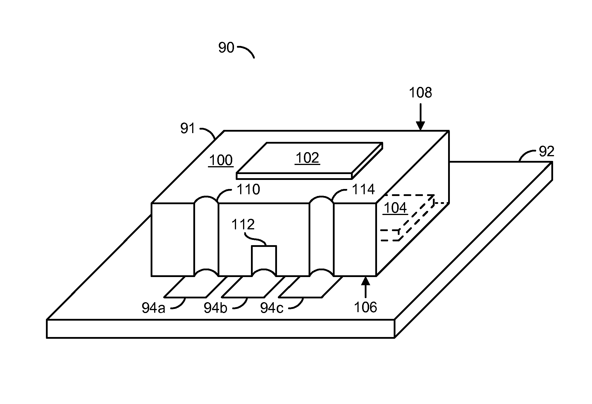
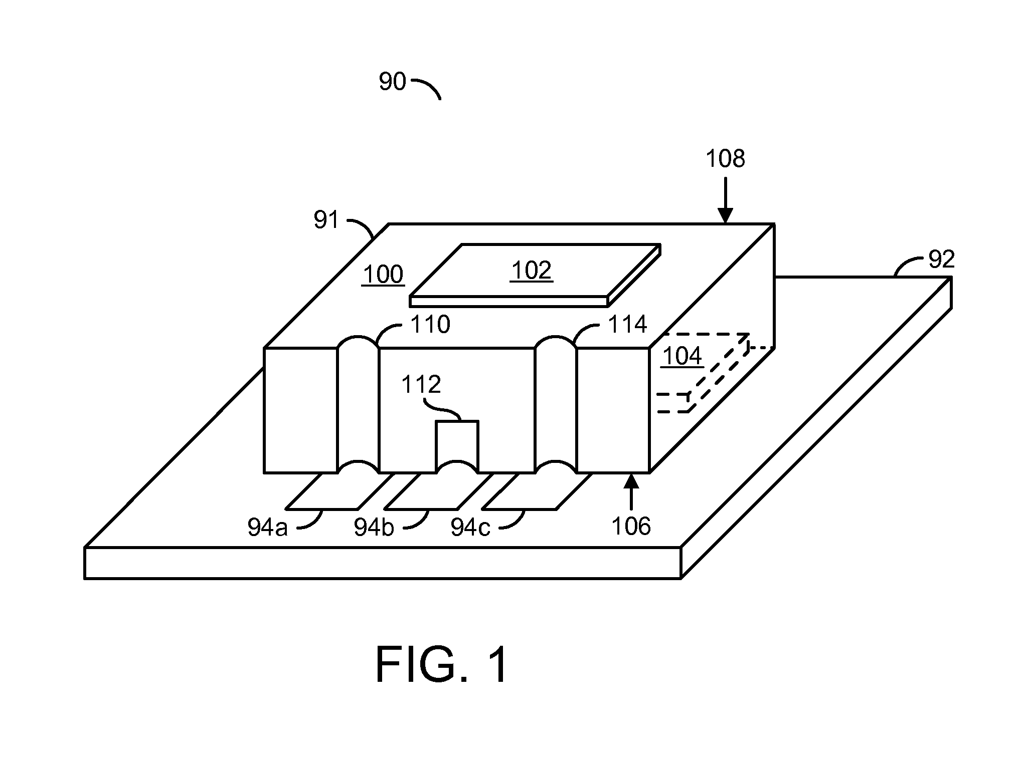
[0013]various embodiments of the invention generally implement one or more blind edge castellations. The blind edge castellations may extend only one or a few conductive layers up from a bottom of a board. Limiting the height of the blind edge castellations generally reduces parasitics that degrade high-frequency signals conveyed by the blind edge castellations. The blind edge castellations may also permit visual inspection of solder joints created between platings in the blind edge castellations and traces on a mother board.

[0014]Referring to FIG. 1, a diagram of an example implementation of a device 90 is shown. The device (or circuit or component) 90 may implement a packaged radio frequency circuit mounted on a mother board. The device 90 generally comprises a board assembly (or substrate or apparatus) 91 and a mother board (or circuit board) 92. The mother board 92 generally comprises multiple traces (or wires) 94a-94c on a top surface. The board assembly 91 generally comprises ...


PUM


Abstract

An apparatus having a plurality of insulating layers, a plurality of conductive layers and a plating is disclosed. The conductive layers may be separated by the insulating layers. A first pattern in a first of the conductive layers generally extends to an edge castellation. A second pattern in a second of the conductive layers may also extends to the edge castellation. The plating may be disposed in the edge castellation and connect the first pattern to the second pattern. The plating in the castellation may extend at most between a subset of the conductive layers.

Description

FIELD OF THE INVENTION[0001]The present invention relates to multilevel circuits generally and, more particularly, to a method and / or apparatus for implementing a blind via edge castellation.BACKGROUND OF THE INVENTION[0002]Conventional land grid array packages often have blind solder joints. Such solder joints cannot be visually inspected and so present a problem. Conventional edge castellations overcome the visual inspection problem by running platings in vias on an outside edge of the package. The solder joints made to the platings are visible. For high-frequency signals used in radio frequency circuits, the edge castellations act like transmission line stubs. Some edge castellations add such sufficient loss to the high-frequency signals that the edge castellations cannot be implemented.[0003]It would be desirable to implement a blind via edge castellation.SUMMARY OF THE INVENTION[0004]The present invention concerns an apparatus having a plurality of insulating layers, a pluralit...

Claims


Application Information

Patent Timeline
Patent Type & Authority Patents(United States)
IPC IPC(8): H05K1/02H05K1/14H05K3/42H05K1/03H05K3/00H05K1/18
CPCH05K1/0237H05K1/0298H05K1/0306H05K3/0094H05K1/14H05K1/181H05K3/429H05K1/0201H05K1/18H01L23/14H05K1/0251H05K1/115H05K1/141H05K3/0097H05K2201/041H05K2201/066H05K2201/09181H05K2201/09509H05K2201/09854H05K2201/10719H01L23/49822H01L23/49805H01L23/13
Inventor WEIGAND, CHRISTOPHER D.ROZBICKI, ANDRZEJ
Owner MACOM TECH SOLUTIONS HLDG INC
Why Eureka
Try Eureka