Methods for forming features in a material layer utilizing a combination of a main etching and a cyclical etching process

a technology of etching and material layer, applied in the direction of basic electric elements, electrical discharge tubes, electrical apparatus, etc., can solve the problems of poor selectivity during etching, bowed, distorted, toppled, or twisted profiles of etched structures, and poor line integrity of formed structures

Active Publication Date: 2017-01-10
APPLIED MATERIALS INC
View PDF65 Cites 110 Cited by
  • Summary
  • Abstract
  • Description
  • Claims
  • Application Information

AI Technical Summary

Problems solved by technology

Reliably producing sub-half micron and smaller features is one of the key technology challenges for next generation very large scale integration (VLSI) and ultra large-scale integration (ULSI) of semiconductor devices.
However, as the limits of circuit technology are pushed, the shrinking dimensions of VLSI and ULSI interconnect technology have placed additional demands on processing capabilities.
Poor process control during etching process will result in irregular structure profiles and line edge roughness, thereby resulting in poor line integrity of the formed structures.
Additionally, irregular profiles and growth of the etching by-products formed during etching may gradually block the small openings used to fabricate the small critical dimension structures, thereby resulting in bowed, distorted, toppled, or twisted profiles of the etched structures.
Furthermore, the similarity between the materials selected for the hardmask layer and the adjacent layers disposed in the film stack, and even the underlying material on the substrate, may also result in similar etch properties therebetween, thereby resulting in poor selectivity during etching.
Poor selectivity between the hardmask layer, adjacent layers and the materials on the substrate may result in non-uniform, tapered and deformed profile of the hardmask layer, thereby leading to poor pattern transfer and failure of accurate structure dimension control.
However, conventional etchants are not selective enough to enable robust manufacturing of next generation devices.

Method used


Image

  • Methods for forming features in a material layer utilizing a combination of a main etching and a cyclical etching process
  • Methods for forming features in a material layer utilizing a combination of a main etching and a cyclical etching process
  • Methods for forming features in a material layer utilizing a combination of a main etching and a cyclical etching process

Examples


Embodiment Construction

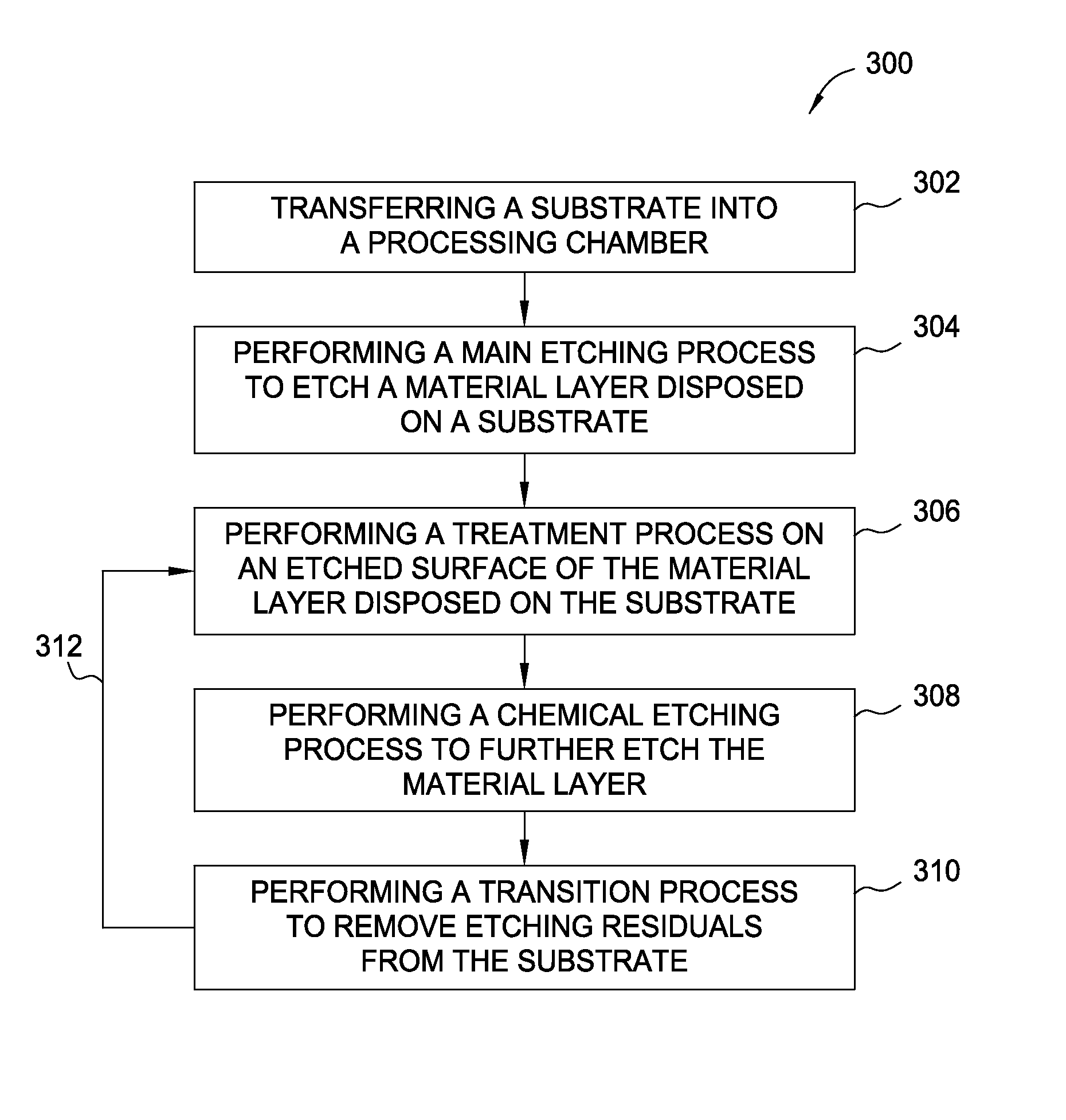
[0020]Embodiments of the present invention provides methods for etching a material layer for high aspect ratio features formed on a substrate for semiconductor devices, with high selectivity and accurate profile control. In one embodiment, the etching process includes using a first step of a main etching process along with a second step of slow cyclical etching process to gradually etch the material layer until the underling substrate is exposed. The slow cyclical etching process may assist controlling the etching selectivity and providing a relatively accurate etch stop endpoint at the interface so as to provide a good profile control for the features formed in the material layer. In one embodiment, the etching process may be utilized to form features, trenches, or vias in a contact dielectric layer for a contact structure for semiconductor devices.

[0021]The term “contact structure” as used herein refers to a layer of material that includes a metal silicide that can form part of a ...


PUM

PropertyMeasurementUnit
temperatureaaaaaaaaaa
frequencyaaaaaaaaaa
diameteraaaaaaaaaa

Abstract

Methods for etching a material layer disposed on the substrate using a combination of a main etching step and a cyclical etching process are provided. The method includes performing a main etching process in a processing chamber to an oxide layer, forming a feature with a first predetermined depth in the oxide layer, performing a treatment process on the substrate by supplying a treatment gas mixture into the processing chamber to treat the etched feature in the oxide layer, performing a chemical etching process on the substrate by supplying a chemical etching gas mixture into the processing chamber, wherein the chemical etching gas includes at least an ammonium gas and a nitrogen trifluoride, wherein the chemical etching process further etches the feature to a second predetermined depth, and performing a transition process on the etched substrate by supplying a transition gas mixture into the processing chamber.

Description

CROSS REFERENCE TO RELATED APPLICATIONS[0001]This application claims benefit of U.S. Provisional Application Ser. No. 61 / 868,037, filed Aug. 20, 2013, which is incorporated by reference in its entirety.BACKGROUND[0002]Field[0003]Embodiments of the present invention generally relate to methods for forming semiconductor devices. More particularly, embodiments of the present invention generally relate to methods for etching a material layer disposed on a substrate using a combination of a main etching and a cyclically etching process for manufacturing semiconductor devices.[0004]Description of the Related Art[0005]Reliably producing sub-half micron and smaller features is one of the key technology challenges for next generation very large scale integration (VLSI) and ultra large-scale integration (ULSI) of semiconductor devices. However, as the limits of circuit technology are pushed, the shrinking dimensions of VLSI and ULSI interconnect technology have placed additional demands on pr...

Claims


Application Information

Patent Timeline
Patent Type & Authority Patents(United States)
IPC IPC(8): H01L21/302H01L21/311H01L21/768
CPCH01L21/31116H01L21/76802H01J2237/334
Inventor LING, MANG-MANGKO, JUNGMINKANG, SEAN S.PENDER, JEREMIAH T.NEMANI, SRINIVAS D.HOWARD, BRADLEY
Owner APPLIED MATERIALS INC
Why Eureka
Try Eureka