Radiation image conversion panel

a technology of conversion panel and radiation image, which is applied in the direction of conversion screen, instruments, nuclear engineering, etc., can solve the problems of insufficient understanding, and achieve the effect of excellent adhesion, excellent luminance and sharpness

Active Publication Date: 2017-01-24
KONICA MINOLTA INC
View PDF11 Cites 1 Cited by
  • Summary
  • Abstract
  • Description
  • Claims
  • Application Information

AI Technical Summary

Benefits of technology

[0015]The radiation image conversion panel of the present invention has a phosphor layer which is crystalline from root portions of columnar crystals and can excellently maintain the adhesion between the phosphors or the like and a support, that is film adhesion.
[0016]Thus, according to the present invention, a radiation image conversion panel excellent in luminance and sharpness can be provided.

Problems solved by technology

Evaluation by the average of X-ray diffractions at the position where effective thickness of sample is relatively large and which is about 10 μm to the thickness direction did not lead to sufficient understanding of the important state in the very early stage of crystal growth.

Method used


Image

  • Radiation image conversion panel
  • Radiation image conversion panel
  • Radiation image conversion panel

Examples


example 1

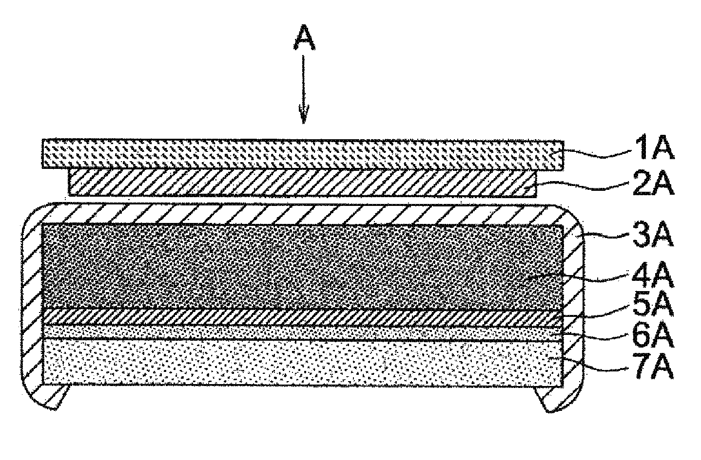
[0128]On a polyimide film (produced by Ube Industries. LTD.; trademark: UPILEX; film thicknesses: 125 μm) as a support, silver as a reflection layer was formed by sputtering method. As an under coating layer, 10 parts by weight of curing agent (HMDI) was blended to 100 parts by weight of polyester (produced by Toyobo Co.; trademark: Vylon 300; glass transition temperature (Tg): 7° C.) and titanium oxide was blended thereto, then 50 parts by weight of toluene and 50 parts by weight of methyl ethyl ketone with respect to 100 parts by weight of solid content were added as a solvent and the mixture was kneaded to obtain a coating solution, which was applied to the polyimide surface by spin coat and dried.

[0129]In this case, the average coating thickness of the under coating layer was 50 μm, and the elastic modulus in a initial substrate temperature measured by nanoindentation method for the under coating layer was 1.1 GPa.

[0130]Cesium iodide and an activator (thallium iodide) were depos...

example 2

[0134]In Example 1, as an under coating layer, 10 parts by weight of curing agent (HMDI) was blended to 100 parts by weight of polyester (produced by Toyobo Co.; trademark: Vylon 780; Tg: 35° C.) and titanium oxide was blended thereto, then 50 parts by weight of toluene and 50 parts by weight of methyl ethyl ketone with respect to 100 parts by weight of solid content were added as a solvent and the mixture was kneaded to obtain a coating solution, which was applied to the polyimide surface by spin coat and dried.

[0135]In this case, the average coating thickness of the under coating layer was 50 μm, and the elastic modulus in a initial substrate temperature measured by nanoindentation method for the under coating layer was 10 GPa.

[0136]A radiation image conversion panel was produced by the same method as in Example 1 except for the above-described and that the initial substrate temperatures was set to 20° C.

example 3

[0137]In Example 1, as an under coating layer, 10 parts by weight of curing agent (HMDI) was blended to 100 parts by weight of polyester (produced by Toyobo Co.; trademark: Vylon 630), then 50 parts by weight of toluene and 50 parts by weight of methyl ethyl ketone with respect to 100 parts by weight of solid content were added as a solvent and the mixture was kneaded to obtain a coating solution, which was applied to the polyimide by spin coat and dried.

[0138]In this case, the average coating thickness of the under coating layer was 1 μm, and the elastic modulus in a initial substrate temperature measured by nanoindentation method for the under coating layer was 6 GPa.

[0139]A radiation image conversion panel was produced by the same method as in Example 1 except for the above-described and that the initial substrate temperatures was set to 50° C.


PUM


Abstract

A radiation image conversion panel having a high luminance and sharpness is provided by growing columnar crystals from the root portion. The radiation image conversion panel includes a support; and a phosphor layer mainly composed of an alkali halide, the phosphor layer being formed by vapor deposition; wherein the phosphor layer includes a plurality of domains formed of a plurality of phosphor columnar crystals; each of the domains is a single phosphor columnar crystal or an aggregation of phosphor columnar crystals having substantially the same crystal orientation, and has an average diameter of 0.2 to 10 μm; and the phosphor columnar crystals are crystalline from root portion at which crystal growth started.

Description

TECHNICAL FIELD[0001]The present invention relates to a radiation image conversion panel.CROSS-REFERENCE TO RELATED APPLICATIONS[0002]To present U.S. patent application claims a priority under the Paris Convention of Japanese patent application No. 2014-188949 filed on Sep. 17, 2014, the entirety of which is incorporated herein by references.BACKGROUND ART[0003]A digital radiation image detector represented by computed radiography (CR) and flat panel detector (FPD) is widely used in diagnostic imaging in hospital and clinic since it can directly obtain digital radiation images and can directly display the images on an image display equipment such as cathode tube and liquid crystal panel. Recently, a FPD utilizing a thin-film transistor (TFT) and a charge-coupled device (CCD) in combination is being popularized.[0004]The FPD comprises a sensor panel (plane light receiving element) in which a light receiving element such as TFT and CCD is arranged two-dimensionally and a radiation ima...

Claims


Application Information

Patent Timeline
Patent Type & Authority Patents(United States)
IPC IPC(8): G21K4/00G01T1/202G01T1/20
CPCG01T1/2012G01T1/2023G21K4/00G21K2004/06G21K2004/12
Inventor MAEDA, KEIKOSHIMA, TETSUO
Owner KONICA MINOLTA INC
Why Eureka
Try Eureka