NAND flash memory and reading method thereof

a reading method and flash memory technology, applied in the direction of digital storage, static storage, instruments, etc., can solve the problems of affecting the miniaturization and high integration of wafers, affecting the accuracy of readings, and presenting following problems

Active Publication Date: 2017-02-07
WINBOND ELECTRONICS CORP
View PDF24 Cites 5 Cited by
  • Summary
  • Abstract
  • Description
  • Claims
  • Application Information

AI Technical Summary

Benefits of technology

[0008]In order to apply a negative voltage to the selected word line, a negative-voltage-generating circuit is usually required. FIG. 2A shows an example of a transistor that is used in the negative-voltage-generating circuit. A negative-voltage generating portion 10 generates a negative voltage, and a N-type metal oxide semiconductor (NMOS) transistor 12 applies the negative voltage to the selected word line. The negative voltage may be, for example, −1 V. Now, if the NMOS transistor is formed within a P-type semiconductor substrate 14 which is applied a voltage of 0 V, a forward bias would be formed between the P-type substrate 14 and the source / drain, which cause the NMOS transistor 12 of such structure to be unable to be used. Hence, as shown in FIG. 2B, it is required to form a N-well 16 within the P-type substrate 14, form a P-well 18 within the N-well 16, and form the NMOS transistor 12 within the P-well 18, so that a reverse bias is existed between the P-well 18 and the N-well 16. The approach of forming such triple-well structure within the substrate can enlarge a distribution area of the negative-voltage-generating circuit, thereby hindering the miniaturization and the high integration of a wafer.

Problems solved by technology

If the maximum voltage difference D is too large, then following problems would be present.
When a memory cell having the lower limit value Min of a threshold value is adjacent to a memory cell having the upper limit value Max of a threshold value, electrical charges of the floating gate of one of the memory cells may cause a capacitive interference to the floating gate of the other memory cell, and thus is hard to perform an accurate reading.
The approach of forming such triple-well structure within the substrate can enlarge a distribution area of the negative-voltage-generating circuit, thereby hindering the miniaturization and the high integration of a wafer.

Method used


Image

  • NAND flash memory and reading method thereof
  • NAND flash memory and reading method thereof
  • NAND flash memory and reading method thereof

Examples


Embodiment Construction

[0028]In the following, embodiments of the disclosure will be described in detail with references to the accompanying drawings. In addition, it is to be noted that, various portions are being emphasised for an ease of understanding, and thus are not illustrated in the same ratios with the actual elements.

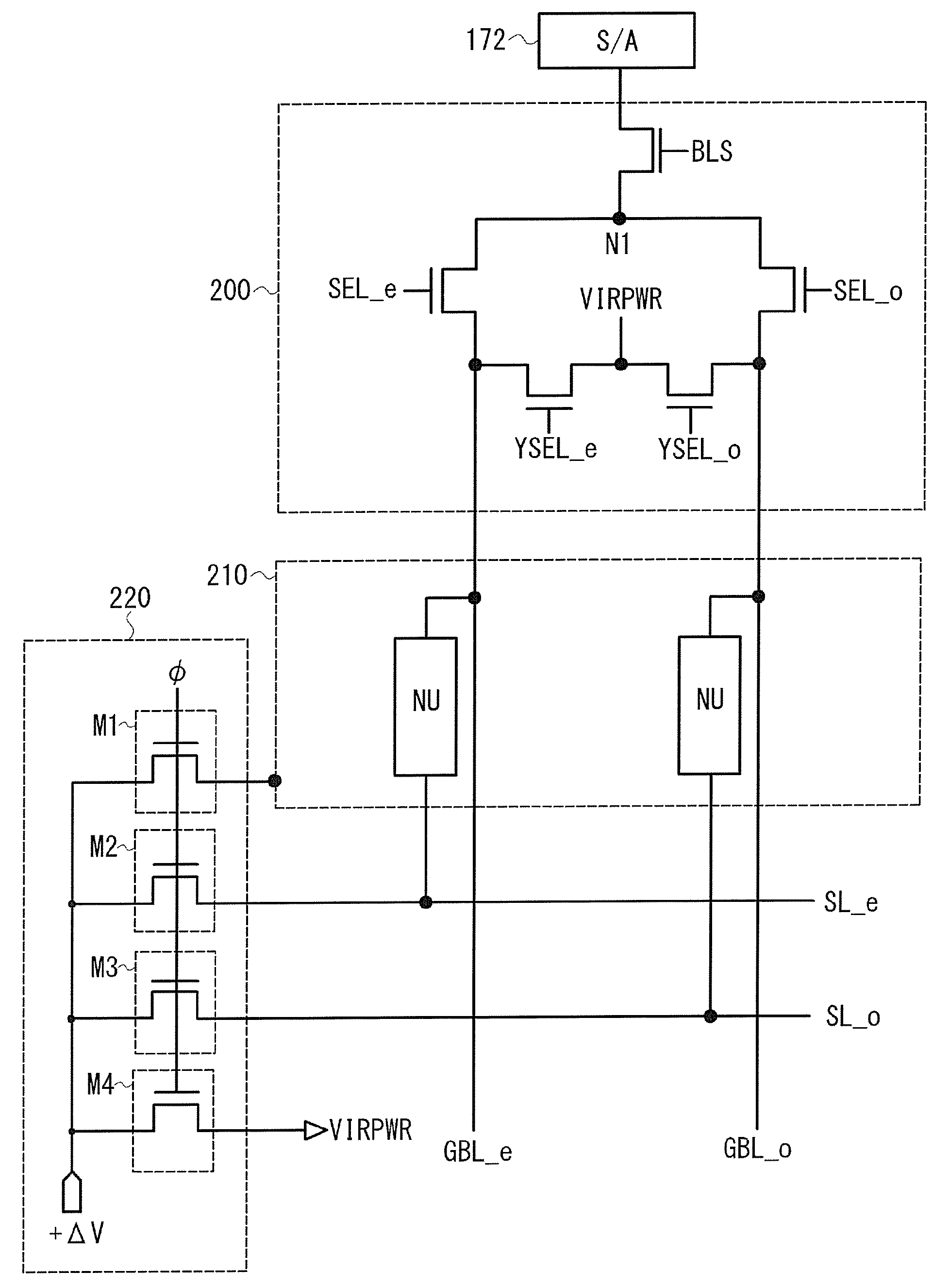
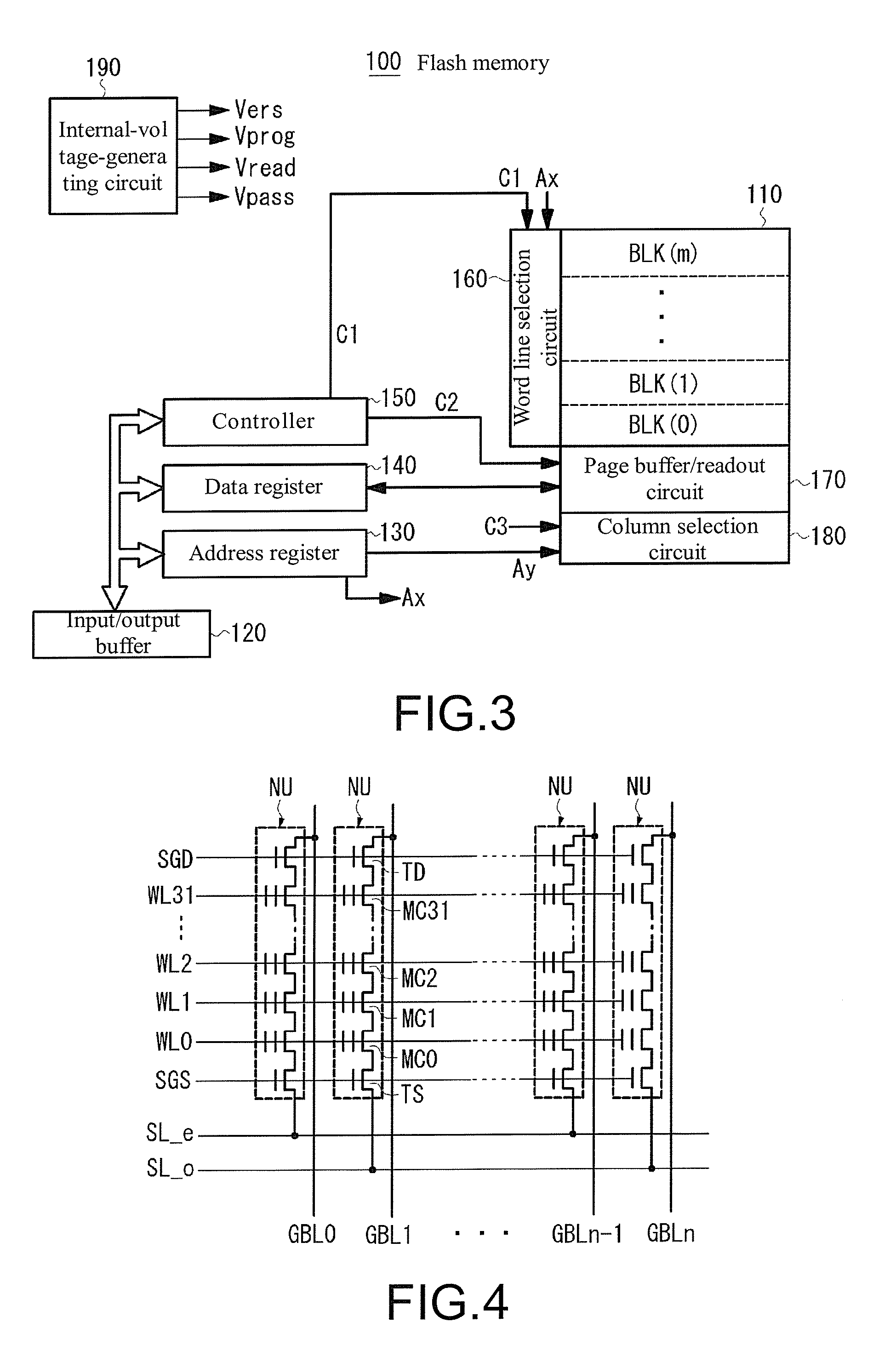
[0029]FIG. 3 illustrates the structure of a NAND flash memory 100 according to an embodiment of the disclosure. As shown in the figure, the flash memory 100 of the present embodiment includes a memory array 110, an input / output buffer 120, an address register 130, a data register 140, a controller 150, a word line selection circuit 160, a page buffer / sense circuit 170, a column selection circuit 180, and an internal-voltage-generating circuit 190. The memory array 110 includes a plurality of memory cells arranged into an array. The input / output buffer 120 is connected to an external input / output terminal I / O. The address register 130 receives address data from the input / output buffe...


PUM


Abstract

The disclosure provides a NAND flash memory and a reading method thereof, which may read a negative threshold value of a memory cell without using a negative-voltage-generating circuit. The disclosed NAND flash memory includes a sense amplifier, a bit line selecting circuit and an array having a plurality of NAND string units. The disclosed NAND flash memory includes a ΔV supplying portion element that applies a positive voltage to a source line, a P well formed with a selected memory cell, and a non-selected bit line which is adjacent to a selected bit line, within a predetermined time period, after the selected bit line is pre-charged and during a reading process.

Description

CROSS-REFERENCE TO RELATED APPLICATION[0001]This application claims the priority benefit of Japan application serial no. 2014-247934, filed on Dec. 8, 2014. The entirety of the above-mentioned patent application is hereby incorporated by reference herein and made a part of this specification.BACKGROUND OF THE DISCLOSURE[0002]1. Field of the Disclosure[0003]The disclosure generally relates to a non-volatile semiconductor memory device and a reading method thereof, and more particularly, to a NAND flash memory and a reading method of a negative threshold voltage of a memory cell of the NAND flash memory.[0004]2. Description of Related Art[0005]A page reading method of a NAND flash memory is performed by alternatively reading pages including even-numbered bit lines or alternatively reading pages including odd-numbered bit lines. When the even-numbered pages are selected, the even-numbered pages are to be connected to a sense amplifier so as to perform the reading of the even-numbered p...

Claims


Application Information

Patent Timeline
Patent Type & Authority Patents(United States)
IPC IPC(8): G11C16/26G11C16/34G11C16/04G11C16/24G11C16/14G11C11/56
CPCG11C16/26G11C16/0483G11C16/3445G11C11/5635G11C11/5642G11C16/14G11C16/24
Inventor SUITO, KATSUTOSHI
Owner WINBOND ELECTRONICS CORP
Why Eureka
Try Eureka