Systems and methods for controlling release of transferable semiconductor structures

a technology of transferable semiconductors and structures, applied in semiconductor devices, semiconductor/solid-state device details, electrical devices, etc., can solve the problems of inability to reliably control active micro-device components, inability to pick up and place ultra-thin or small micro-devices using this technology, and conventional micro-transfer printing techniques lack the reproducibility and precision required to efficiently produce electronics with high-density devices at low cost. , to achieve the effect of improving the removal of a

Active Publication Date: 2017-03-21
X DISPLAY CO TECH LTD
View PDF75 Cites 112 Cited by
  • Summary
  • Abstract
  • Description
  • Claims
  • Application Information

AI Technical Summary

Benefits of technology

[0010]The disclosed technology relates generally to systems and methods for controlling the release of micro devices using tethers from a native substrate. The disclosed technology provides reliably controlled and predictable release of micro-device components from a substrate, leading to efficiencies, reproducibilities, and less errors during micro-assembly. In certain embodiments, the disclosed technology accomplishes this using a single, off-center tether per micro-device. As described herein, this improves the removal of a sacrificial layer. For example, in some embodiments, this improves the etching of the sacrificial layer such that the desired area under the micro-device is removed in its entirety so that the micro-device can be micro-assembled (e.g., the micro-device can be picked up by a elastomer stamp causing the tether to break).

Problems solved by technology

It is often difficult to pick up and place ultra-thin or small micro devices using this technology.
However, conventional micro transfer printing techniques lack the reproducibility and precision required to efficiently produce electronics with high-density devices at low cost.
However, it has been demonstrated that the release of the active micro-device components is not reliably controlled and not predictable, leading to inefficiencies, irreproducibilities, and errors.

Method used


Image

  • Systems and methods for controlling release of transferable semiconductor structures
  • Systems and methods for controlling release of transferable semiconductor structures
  • Systems and methods for controlling release of transferable semiconductor structures

Examples


Embodiment Construction

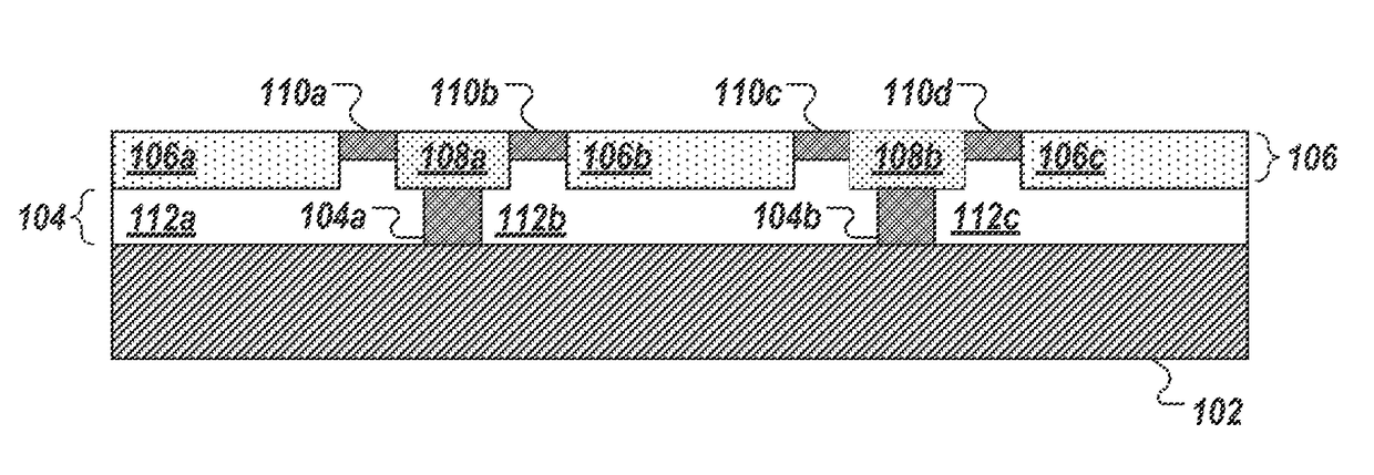
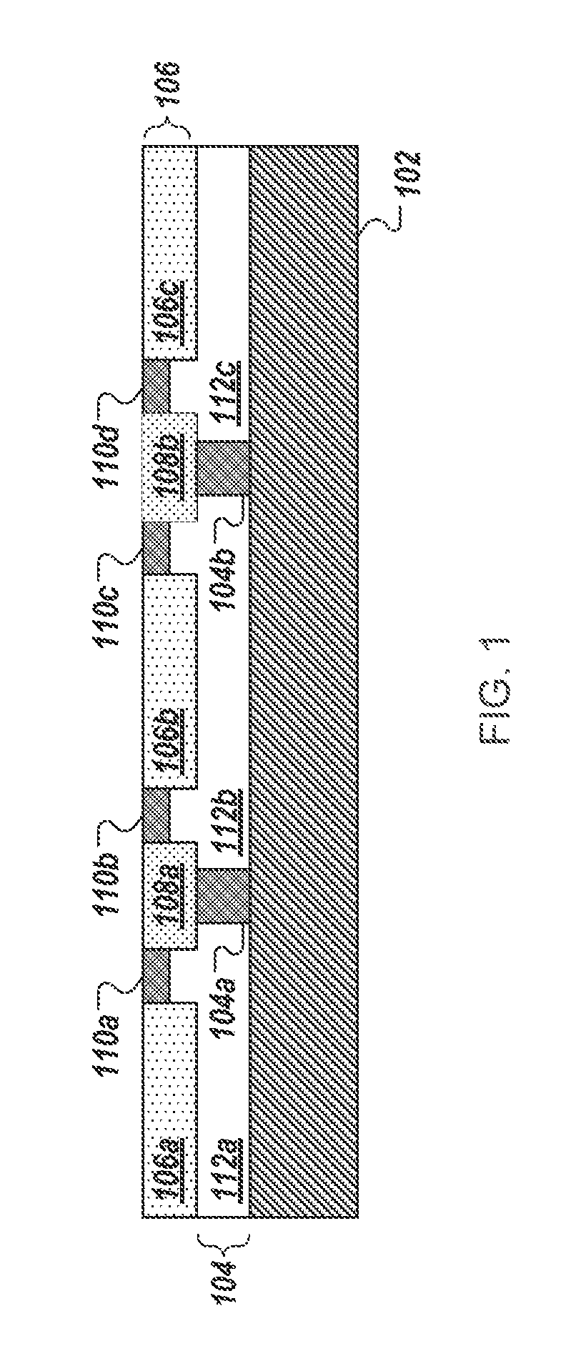
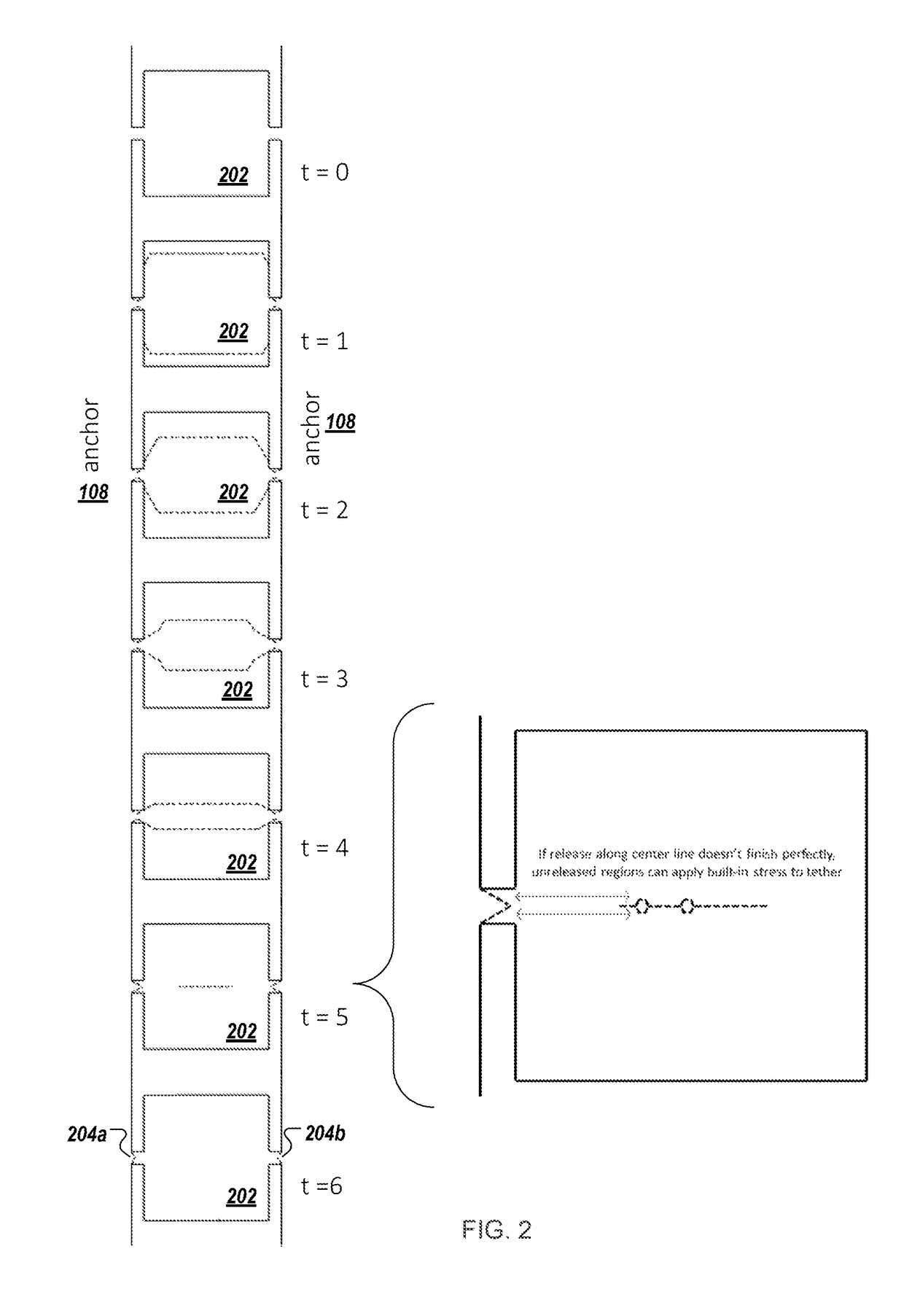
[0087]As used herein the expression “semiconductor element” and “semiconductor structure” are used synonymously and broadly refer to a semiconductor material, structure, device, or component of a device. Semiconductor elements include high-quality single crystalline and polycrystalline semiconductors, semiconductor materials fabricated via high-temperature processing, doped semiconductor materials, organic and inorganic semiconductors, and composite semiconductor materials and structures having one or more additional semiconductor components and / or non-semiconductor components, such as dielectric layers or materials and / or conducting layers or materials. Semiconductor elements include semiconductor devices and device components including, but not limited to, transistors, photovoltaics including solar cells, diodes, light-emitting diodes, lasers, p-n junctions, photodiodes, integrated circuits, and sensors. In addition, semiconductor element can refer to a part or portion that forms ...


PUM

PropertyMeasurementUnit
widthaaaaaaaaaa
widthaaaaaaaaaa
widthaaaaaaaaaa

Abstract

The disclosed technology relates generally to methods and systems for controlling the release of micro devices. Prior to transferring micro devices to a destination substrate, a native substrate is formed with micro devices thereon. The micro devices can be distributed over the native substrate and spatially separated from each other by an anchor structure. The anchors are physically connected / secured to the native substrate. Tethers physically secure each micro device to one or more anchors, thereby suspending the micro device above the native substrate. In certain embodiments, single tether designs are used to control the relaxation of built-in stress in releasable structures on a substrate, such as Si (1 1 1). Single tether designs offer, among other things, the added benefit of easier break upon retrieval from native substrate in micro assembly processes. In certain embodiments, narrow tether designs are used to avoid pinning of the undercut etch front.

Description

RELATED APPLICATIONS[0001]This application claims priority to and the benefit of U.S. Provisional Patent Application No. 62 / 014,078, filed Jun. 18, 2014, titled “Systems and Methods for Controlling Release of Transferable Semiconductor Structures,” and U.S. Provisional Patent Application No. 62 / 029,535, filed Jul. 27, 2014, titled “Systems and Methods for Controlling Release of Transferable Semiconductor Structures,” the content of each of which is incorporated by reference herein in their entirety.FIELD OF THE INVENTION[0002]The disclosed technology relates generally to systems and methods for controlling the release of micro devices using tethers from a native substrate.BACKGROUND OF THE INVENTION[0003]The disclosed technology relates generally to the formation of transferable micro devices. Semiconductor chip- or die-automated assembly equipment typically uses vacuum-operated placement heads, such as vacuum grippers or pick-and-place tools, to pick up and apply devices to a subst...

Claims


Application Information

Patent Timeline
Patent Type & Authority Patents(United States)
IPC IPC(8): H01L21/56B81C99/00H01L21/683H01L23/00
CPCH01L21/561B81C99/008H01L21/6835H01L21/6836H01L24/83H01L21/568H01L2221/68368H01L21/7813
Inventor BOWER, CHRISTOPHERMEITL, MATTHEW
Owner X DISPLAY CO TECH LTD
Why Eureka
Try Eureka