Eureka AIR delivers breakthrough ideas for toughest innovation challenges, trusted by R&D personnel around the world.

Mold release film and process for producing semiconductor package

a technology of mold release film and semiconductor package, which is applied in the direction of packaging foodstuffs, packaged goods types, synthetic resin layered products, etc., can solve the problems of poor appearance, easy formation of wrinkles in the mold release film, and hardly releasable proportions, so as to improve the productivity of the semiconductor package, improve the followability to the mold, and improve the effect of the semiconductor packag

Active Publication Date: 2017-04-04
ASAHI GLASS CO LTD
View PDF22 Cites 5 Cited by
  • Summary
  • Abstract
  • Description
  • Claims
  • Application Information

AI Technical Summary

Benefits of technology

[0045]The mold release film of the present invention is unlikely to have wrinkles or pinholes formed when the mold release film is brought in close contact with the cavity surface of the mold in the encapsulation step of forming a resin-encapsulation portion by encapsulating a semiconductor element with a curable resin. Further, when the thickness is made to be from 40 to 75 μm, it is particularly excellent in the followability to the mold. Therefore, according to the mold release film of the present invention, poor appearance of the resin-encapsulation portion or adhesion of the curable resin to the mold in the encapsulation step is unlikely to occur, and it is possible to improve the productivity of the semiconductor package.
[0046]In the process for producing a semiconductor package of the present invention, in the encapsulation step of forming the resin-encapsulation portion by encapsulating a semiconductor element with a curable resin, wrinkles or pinholes are unlikely to be formed when the mold release film is brought in close contact with the cavity surface of the mold. Further, when the thickness of the mold release film is made to be from 40 to 75 μm, the followability to the mold will be especially excellent. Therefore, poor appearance of the resin-encapsulation portion or adhesion of the curable resin to the mold in the encapsulation step is unlikely to occur. Thus, according to the process for producing a semiconductor package of the present invention, it is possible to produce a semiconductor package with good productivity.
[0047]Further, at the time of forming an ink layer by printing with an ink on the surface of the resin-encapsulation portion, chipping or cracking is unlikely to occur in the singulation step, and it is possible to form a resin-encapsulation portion excellent in adhesion to the ink layer.
[0048]Further, in the process for producing a semiconductor package of the present invention, it is possible to prevent chipping or cracking of the resin-encapsulation portion in the singulation step. Also, it is possible to form an ink layer with good adhesion on the resin-encapsulation portion. Thus, according to the process for producing a semiconductor package of the present invention, it is possible to produce a semiconductor package having no chipping or cracking in the resin-encapsulation portion, whereby the ink layer is unlikely to be peeled.

Problems solved by technology

Especially in a case where a plurality of semiconductor elements are collectively encapsulated, as compared with the case of encapsulating one semiconductor element in one cavity, the cavity tends to be large-sized and complicated so that the resin-encapsulation portion tends to be hardly releasable, and therefore, a mold release film is used in many cases.
At that time, however, if the mold release film is brought in contact with the cavity surface in such a state that air is not yet completely evacuated during stretching, air spaces may partly be formed between the mold release film and the cavity surfaces, and wrinkles are likely to be formed in the mold release film at such portions.
If the mold release film has wrinkles, the shape of such wrinkles on the mold release film is likely to be transferred to the surface of the resin-encapsulation portion, thus leading to poor appearance, whereby the yield will be lowered.

Method used


Image

  • Mold release film and process for producing semiconductor package
  • Mold release film and process for producing semiconductor package
  • Mold release film and process for producing semiconductor package

Examples


first embodiment

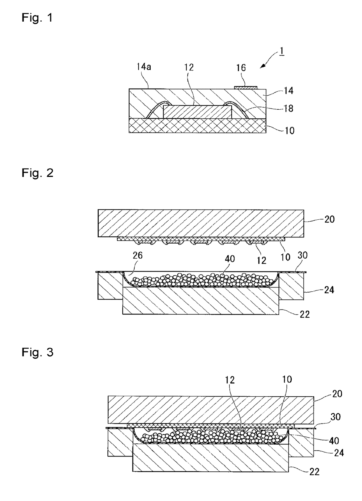
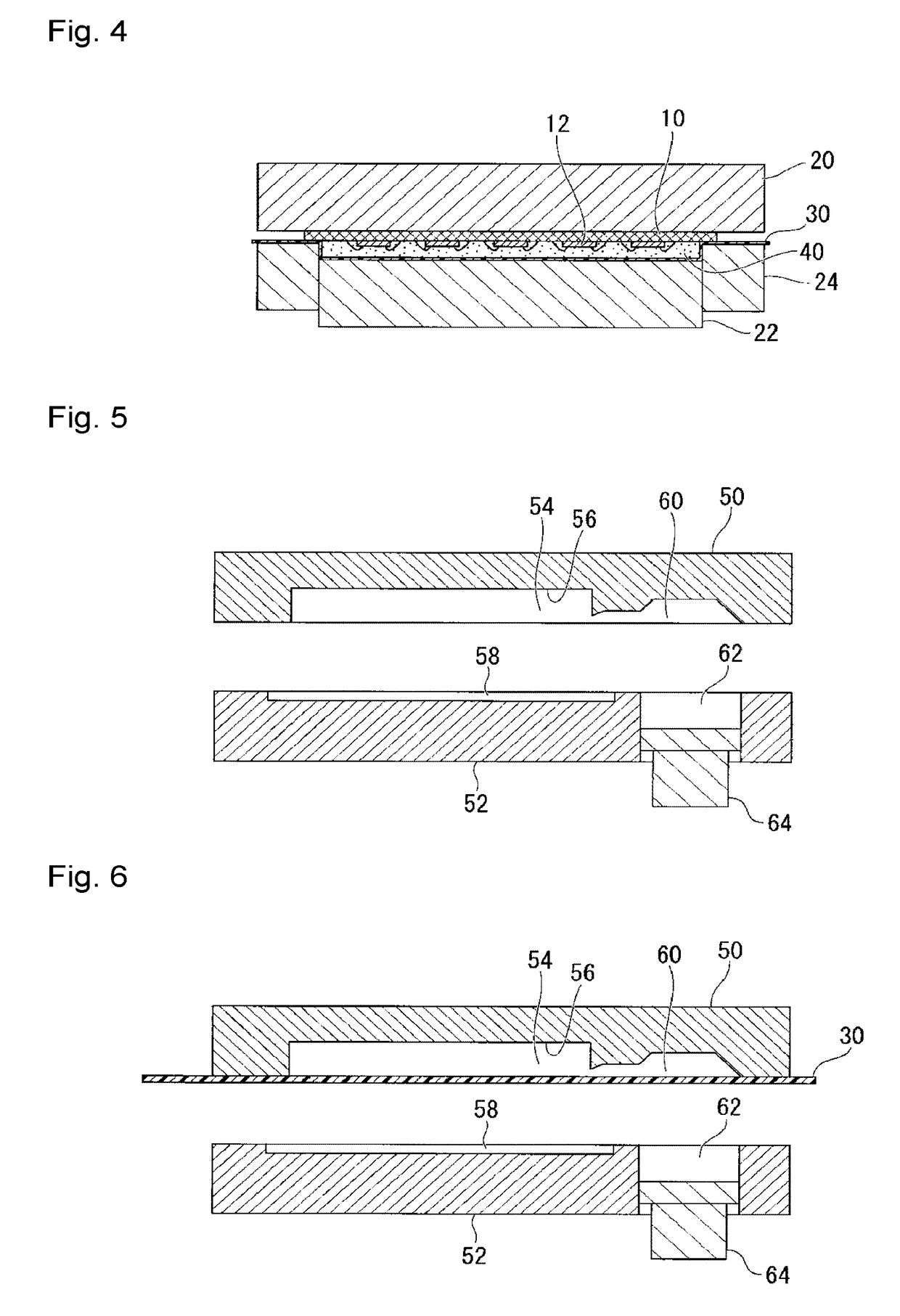
[0248]As one embodiment of the process for producing a semiconductor package, a case of producing a semiconductor package 1 as shown in FIG. 1 by the process (α), will be described in detail.

Mold:

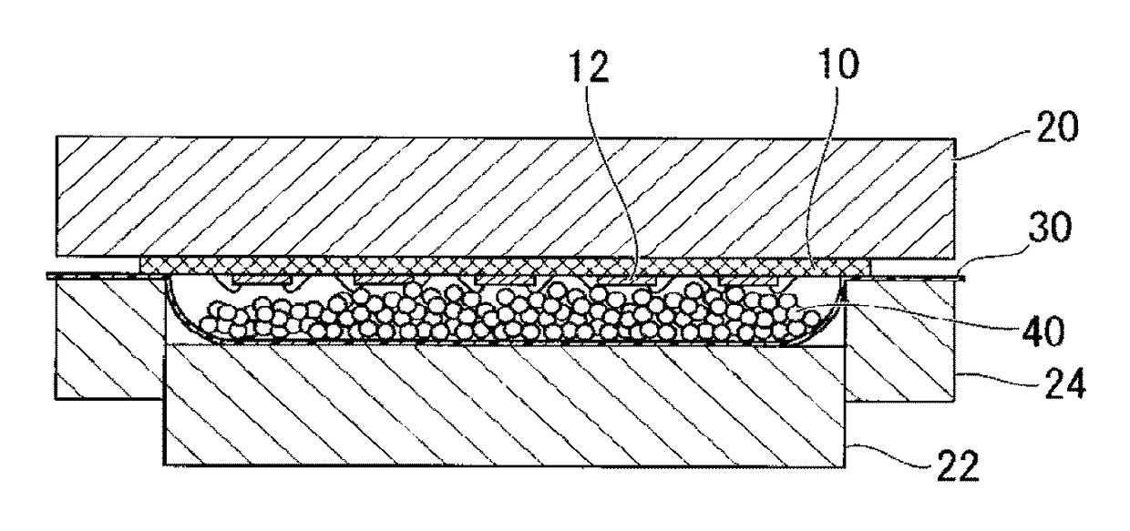
[0249]As the mold in the first embodiment, it is possible to use one known as a mold to be used for compression molding, and for example, as shown in FIG. 2, a mold comprising a stationary upper mold 20, a cavity bottom member 22, and a frame-shaped movable lower mold 24 disposed at the periphery of the cavity bottom member 22, may be mentioned.

[0250]In the stationary upper mold 20, a vacuum vent (not shown) for adsorbing a substrate 10 to the stationary upper mold 20 by sucking air between the substrate 10 and the stationary upper mold 20, is formed. Further, in the cavity bottom member 22, a vacuum vent (not shown) for adsorbing a mold release film 30 to the cavity bottom member 22 by sucking air between the mold release film 30 and the cavity bottom member 22, is formed.

[0251]In this mol...

second embodiment

[0289]Another embodiment of the process for producing a semiconductor package will be described in detail with reference to a case of producing a semiconductor package 1 shown in FIG. 1 by the process (β).

Mold:

[0290]As the mold in the second embodiment, it is possible to use one known as a mold to be used for a transfer molding method. For example, as shown in FIG. 5, a mold comprising an upper mold 50 and a lower mold 52, may be mentioned. In the upper mold 50, a cavity 54 having a shape corresponding to the shape of the resin-encapsulation portion 14 to be formed in the step (β4), and a concave-shaped resin-introducing portion 60 to introduce a curable resin 40 to the cavity 54 are formed. In the lower mold 52, a substrate placement portion 58 for placing a substrate 10 having semiconductor chips 12 mounted thereon, and a resin placement portion 62 for placing a curable resin 40 are formed. Further, in the resin placement portion 62, a plunger 64 is provided that pushes the curabl...

production example 1

Production of ETFE (1)

[0321]A polymerization tank having an internal capacity of 1.3 L and equipped with a stirrer, was deaerated; 881.9 g of 1-hydrotridecafluoro-hexane, 335.5 g of 1,3-dichloro-1,1,2,2,3-pentafluoropropane (trade name “AK225cb” manufactured by Asahi Glass Company, Ltd., hereinafter referred to as AK225cb) and 7.0 g of CH2═CHCF2CF2CF2CF3 (PFBE), were charged; 165.2 g of TFE and 9.8 g of ethylene (hereinafter referred to as E) were injected; the temperature in the polymerization tank was raised to 66° C.; and as a polymerization initiator solution, 7.7 mL of an AK225cb solution containing 1 mass % of tert-butyl peroxypivalate (hereinafter referred to as PBPV) was charged to initiate the polymerization.

[0322]A monomer mixture gas of TFE / E=54 / 46 by molar ratio was continuously charged so that the pressure would be constant during the polymerization. Further, along with the charging of the monomer mixture gas, PFBE was continuously charged in an amo...


PUM

PropertyMeasurementUnit
Raaaaaaaaaaa
thicknessaaaaaaaaaa
thicknessaaaaaaaaaa

Abstract

A mold release film to be disposed on a cavity surface of a mold in a method for producing a semiconductor package wherein a semiconductor element is disposed in the mold and encapsulated with a curable resin to form a resin-encapsulation portion, characterized in that it has a first surface to be in contact with the curable resin at the time of forming the resin-encapsulation portion, and a second surface to be in contact with the cavity surface, at least one of the first surface and the second surface has irregularities formed thereon, and the surface having irregularities formed thereon, has an arithmetic mean roughness (Ra) of from 1.3 to 2.5 μm and a peak count (RPc) of from 80 to 200; and a process for producing a semiconductor package by using the mold release film.

Description

TECHNICAL FIELD[0001]The present invention relates to a mold release film to be disposed on a cavity surface of a mold in a method for producing a semiconductor package wherein a semiconductor element is disposed in a mold and encapsulated with a curable resin to form a resin-encapsulation portion, and a process for producing a semiconductor package by using the mold release film.BACKGROUND ART[0002]A semiconductor package has a resin-encapsulation portion to protect a semiconductor element. For formation of the resin-encapsulation portion (for encapsulation of a semiconductor element), a curable resin e.g. a thermosetting resin such as an epoxy resin is used.[0003]As a method for producing a semiconductor package, for example, a method comprising an encapsulating step by a so-called compression molding method or transfer molding method is known, wherein a substrate having a semiconductor element mounted thereon, is disposed so that the semiconductor element is located at a predeter...

Claims


Application Information

Patent Timeline
Patent Type & Authority Patents(United States)
IPC IPC(8): H01L21/56B29C33/68B32B7/06H01L23/00B32B27/32B32B3/28B29C43/18B29C48/08B29C48/305B29L31/34
CPCB29C43/18B32B3/28B32B7/06B32B27/322H01L21/565H01L24/97H01L21/566B29C33/68B29L2031/3406B32B2307/748B32B2439/00H01L2224/48091H01L2224/73265H01L2924/181H01L2924/00014H01L2924/00012B29C48/08
Inventor KASAI, WATARUSUZUKI, MASAMI
Owner ASAHI GLASS CO LTD
Why Eureka
Eureka Blog
Learn More