Programmable circuits for correcting scan-test circuitry defects in integrated circuit designs

a technology of integrated circuits and scan-test circuits, applied in the field of electronic devices, can solve problems such as scan-chain defects that can occur, high difficulty in meeting requirements, and scan-chain defects that cannot be corrected

Active Publication Date: 2017-04-11
LATTICE SEMICON CORP
View PDF7 Cites 127 Cited by
  • Summary
  • Abstract
  • Description
  • Claims
  • Application Information

AI Technical Summary

Problems solved by technology

Sometimes, it is highly challenging to meet these requirements (particularly on designs with multiple functional clock domains) due to the design complexity, design revisions late in the design cycle, and the time-to-market pressure.
Although a scan chain is designed to support scan testing to determine whether there are any defects in the CUST, the fact is that there may be defects in the scan chain itself.
There are a number of different types of scan-chain defects that can occur along a scan chain.
Such timing skew may result due to incorrect timing constraints used during static timing analysis or by the failure of the place-and-route tool to close timing with the correct timing constraints.
In that case, a hold-time violation will occur which may result in a loss of data.
This design modification may involve making mask revisions, which typically requires a backend design engineer to successfully close timing in scan-test mode and correct all the other design problems that cause scan-test problems, and is therefore very time consuming and costly in terms of non-recurring engineering (NRE) resources and mask costs.
Even if this problem is detected before chip manufacture (thereby avoiding costly mask revisions), the time-to-market pressure makes it highly challenging and expensive to correct timing and logical problems that occur in scan-test mode due to late design revisions.
If the particular polarity of the lockup latch 340 does not match the presence / absence of the inverter 350, then a polarity-reversal scan-chain defect will exist, and the scan chain might not operate properly.
Here, too, such modification may involve making costly and time-consuming mask revisions.
Another situation where a polarity-reversal defect can occur in scan-test circuitry is when a scan-test control signal or other constrained scan-test input signal of the wrong polarity is applied to scan-test control circuitry that controls the scan testing within an integrated circuit.
If, for some reason, the constrained signal 405 has the wrong polarity, then the scan testing of the CUST implemented by the scan-test control circuitry 410 may be improper.
This can significantly increase both the time and cost of designing integrated circuits.

Method used


Image

  • Programmable circuits for correcting scan-test circuitry defects in integrated circuit designs
  • Programmable circuits for correcting scan-test circuitry defects in integrated circuit designs
  • Programmable circuits for correcting scan-test circuitry defects in integrated circuit designs

Examples


Embodiment Construction

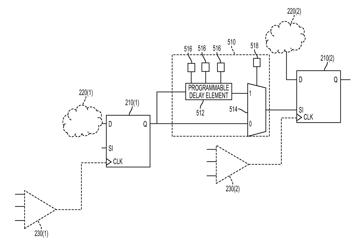
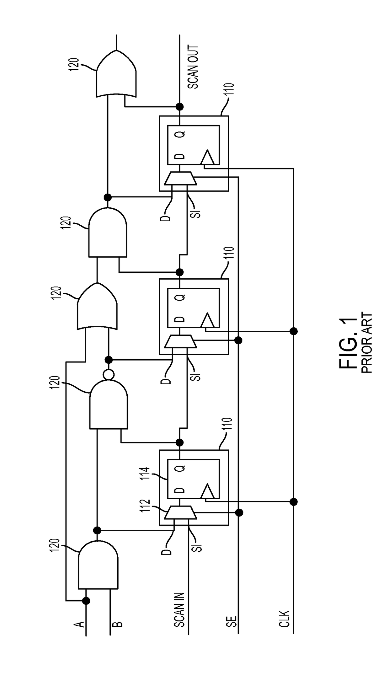
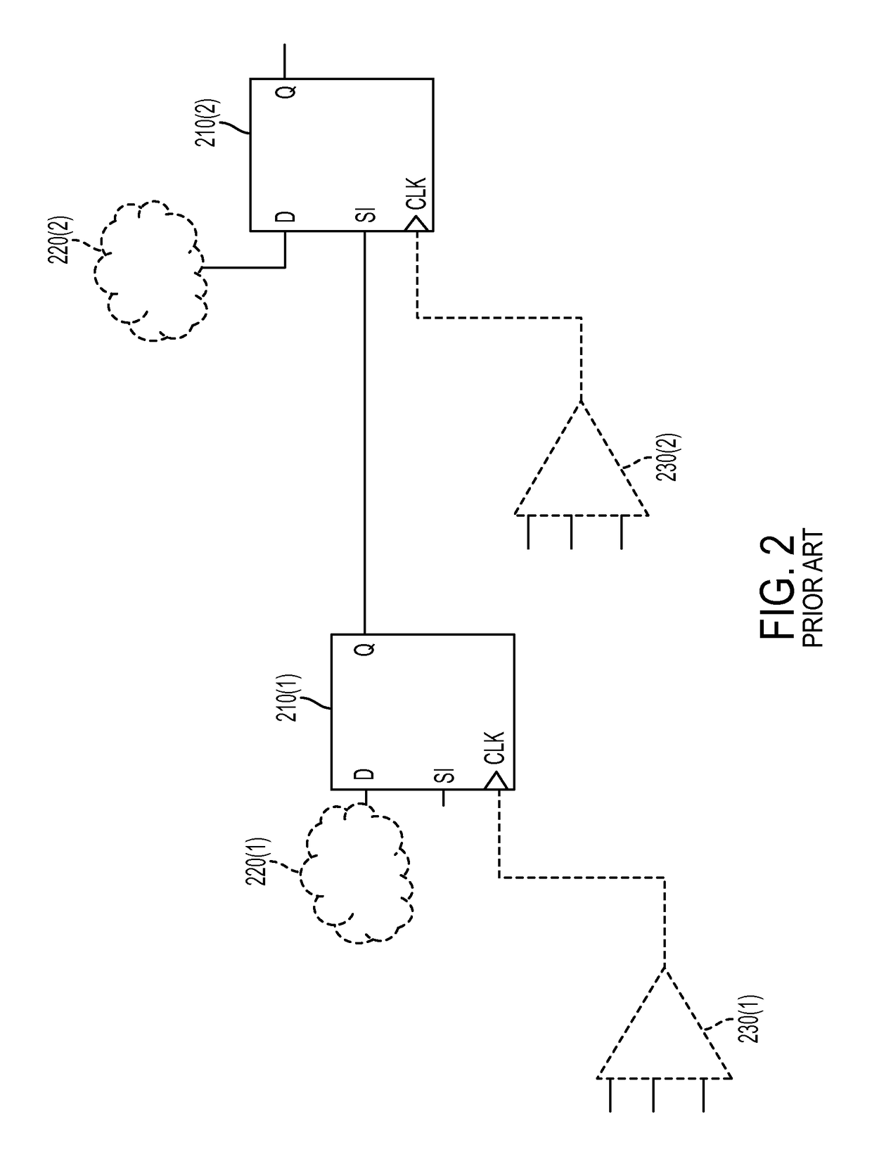
[0028]Detailed illustrative embodiments of the present invention are disclosed herein. However, specific structural and functional details disclosed herein are merely representative for purposes of describing example embodiments of the present invention. The present invention may be embodied in many alternate forms and should not be construed as limited to only the embodiments set forth herein. Further, the terminology used herein is for the purpose of describing particular embodiments only and is not intended to be limiting of example embodiments of the invention.

[0029]As used herein, the singular forms “a,”“an,” and “the,” are intended to include the plural forms as well, unless the context clearly indicates otherwise. It further will be understood that the terms “comprises,”“comprising,”“includes,” and / or “including,” specify the presence of stated features, steps, or components, but do not preclude the presence or addition of one or more other features, steps, or components. It ...


PUM


Abstract

In certain embodiments, an integrated circuit has scan-test circuitry that performs scan testing on circuitry under scan test (CUST) within the IC, where the scan-test circuitry is susceptible to a defect. In order to enable the defect to be corrected after it occurs, the scan-test circuitry includes a set of programmable circuitry connected to provide a signal to other circuitry (e.g., a scan chain) within the scan-test circuitry, where the set of programmable circuitry includes one or more configurable memory cells connected to control the programming of the set of programmable circuitry. The memory cell(s) can be configured to program the set of programmable circuitry to enable the scan testing to be performed without modification. The memory cell(s) can also be configured to program the set of programmable circuitry to modify the scan testing to correct the defect in the scan-test circuitry.

Description

BACKGROUND[0001]Field of the Invention[0002]The present invention relates to electronics and, more specifically but not exclusively, to integrated circuits having defects in their scan-test circuitry, including, but not limited to, scan-chain defects.[0003]Description of the Related Art[0004]This section introduces aspects that may help facilitate a better understanding of the invention. Accordingly, the statements of this section are to be read in this light and are not to be understood as admissions about what is prior art or what is not prior art.[0005]It is well known to design an integrated circuit (IC), such as (without limitation) a field-programmable gate array (FPGA), with scan-test circuitry that supports scan testing of the integrated circuitry to detect defects in the functionality of that integrated circuitry. Scan testing typically involves synthesizing scan chains in hard logic blocks embedded in the integrated circuit by replacing regular flip-flop cells with scan fl...

Claims


Application Information

Patent Timeline
Patent Type & Authority Patents(United States)
IPC IPC(8): G06F11/22G01R31/3177G01R31/317G06F17/50
CPCG01R31/3177G01R31/3172G01R31/318588G01R31/318536
Inventor CHAKRABORTY, KANAD
Owner LATTICE SEMICON CORP
Why Eureka
Try Eureka