Thin film transistor, array substrate and display device

a thin film transistor and array substrate technology, applied in the field of display technology, can solve the problems of large subthreshold swing of tft, serious impact on and reduce the oxygen vacancies in the active layer, and improve the operation capacity of tft. , the effect of increasing the transmission rate of carriers

Active Publication Date: 2017-04-11
BOE TECH GRP CO LTD
View PDF7 Cites 0 Cited by
  • Summary
  • Abstract
  • Description
  • Claims
  • Application Information

AI Technical Summary

Benefits of technology

[0018]The benefit effects of the invention are as follows. In the thin film transistor provided by the invention, with the oxygen vacancy reducing layer, the number of the oxygen vacancies in the active layer is reduced significantly, thereby the transmission rate of the carriers is increased while the subthreshold swing of TFT is decreased, resulting in improved operation capacity of TFT. Furthermore, contact characteristic between the source and / or drain and the active layer may be improved by improving work function of the oxygen vacancy reducing layer. In other words, contact resistance(s) between the source and / or drain and the active layer may be decreased significantly, and thus the transmission rate of the carriers may be further improved.
[0019]In the array substrate of the invention, with the above thin film transistor employed, the performance of the array substrate can be improved. In the display device of the invention, with the above array substrate employed, the performance of the display device can be improved.

Problems solved by technology

The increased subthreshold swing may impact on operation capacity of TFT seriously.
In addition, contact resistances between the active layer and the source, the drain are usually large, which also impacts on the transmission of the carriers, resulting in larger subthreshold swing of TFT, and thereby impacting on operation capacity of TFT seriously.

Method used


Image

  • Thin film transistor, array substrate and display device
  • Thin film transistor, array substrate and display device
  • Thin film transistor, array substrate and display device

Examples


embodiment 1

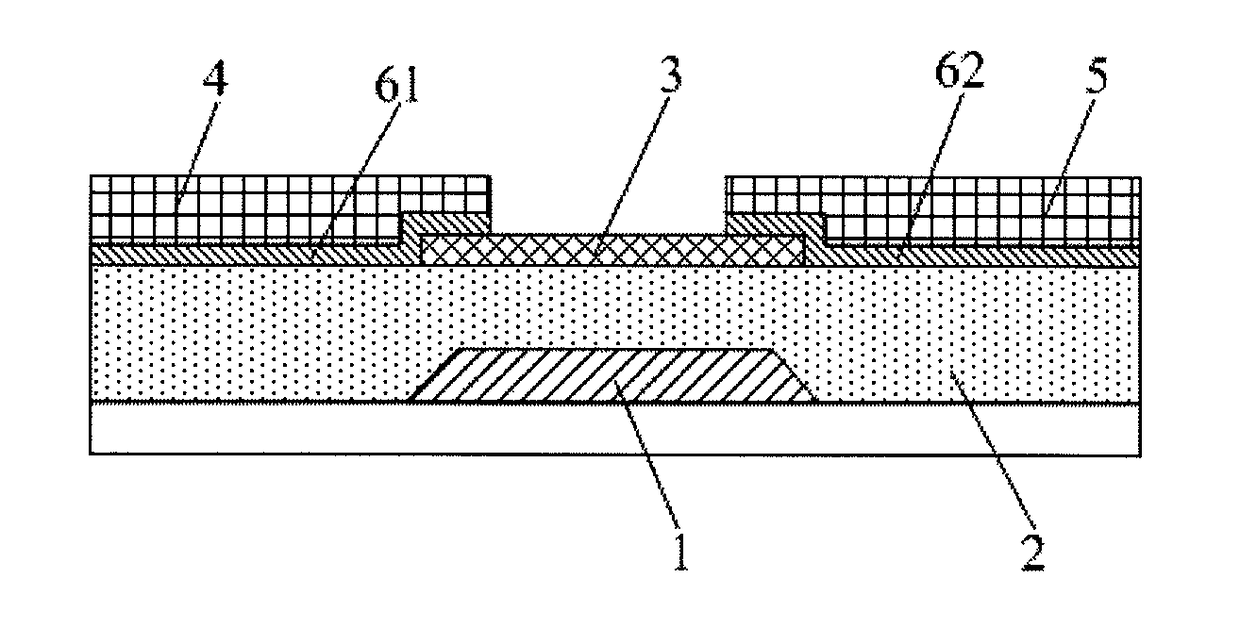
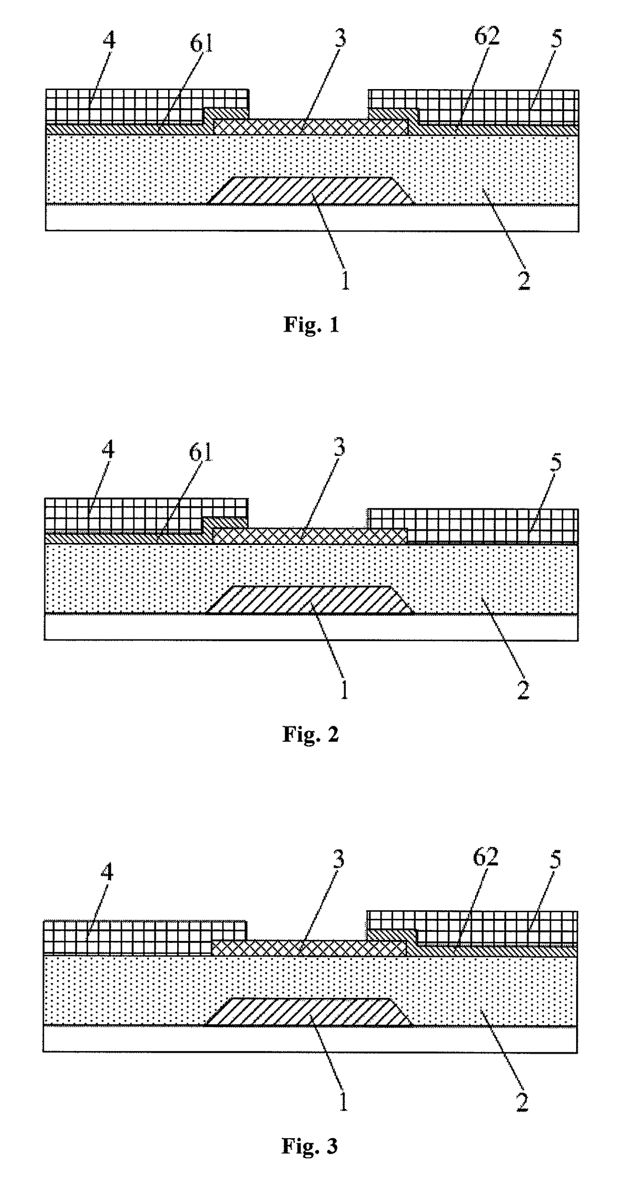
[0027]The present embodiment provides a thin film transistor which, as shown in FIG. 1, comprises a gate 1, a gate insulation layer 2, an active layer 3, a source 4 and a drain 5. The gate insulation layer 2 is disposed between the gate 1 and the active layer 3 so as to insulate the gate 1 from the active layer 3. The source 4 and the drain 5 are disposed at two ends of the active layer 3, respectively. The active layer 3 is formed by using material of metallic nitrogen-oxide. The thin film transistor further comprises a conductive oxygen vacancy reducing layer for decreasing oxygen vacancies in the active layer 3. In this embodiment, the oxygen vacancy reducing layer is disposed between the active layer 3 and the source 4, and between the active layer 3 and the drain 5.

[0028]The material of metallic nitrogen-oxide may be zinc gallium oxynitride, zinc indium oxynitride, zinc aluminum oxynitride, zinc oxynitride (ZnON), and the like.

[0029]In this embodiment, the oxygen vacancy reduci...

embodiment 2

[0037]The present embodiment provides a thin film transistor, which is different from that of embodiment 1 in that the oxygen vacancy reducing layer in this embodiment comprises only the first reducing part 61 (as shown in FIG. 2) or only the second reducing part 62 (as shown in FIG. 3).

[0038]Accordingly, when preparing the thin film transistor shown in FIG. 2, a pattern including the first reducing part 61 is formed by a single patterning process at first, and then a pattern including the source 4 and the drain 5 is formed by another single patterning process. When preparing the thin film transistor shown in FIG. 3, a pattern including the second reducing part 62 is formed by a single patterning process at first, and then a pattern including the source 4 and the drain 5 is formed by another single patterning process.

[0039]Except that the thin film transistor of this embodiment is provided with the oxygen vacancy reducing layer, other structures as well as materials for components i...

embodiment 3

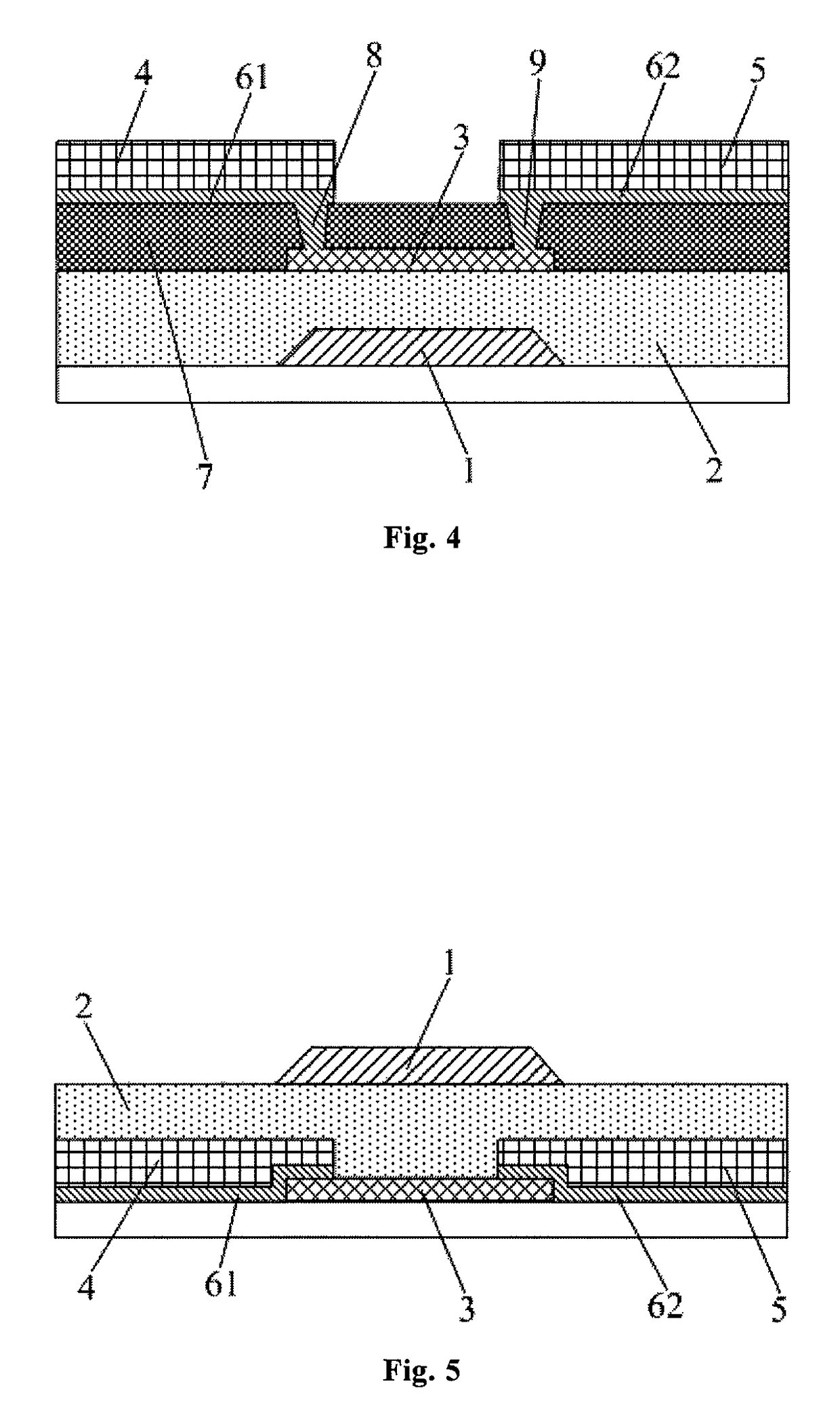
[0041]The present embodiment provides a thin film transistor which is different from those in Embodiments 1 and 2 in that, as shown in FIG. 4, the thin film transistor further comprises a etch stopping layer 7 which is disposed between the active layer 3 and the source 4 and drain 5. The oxygen vacancy reducing layer is located at a side of the etch stopping layer 7 away from the active layer 3. A first via 8 is opened within a region of the etch stopping layer 7 in which the first reducing part 61 is located so that the first reducing part 61 is contacted with the active layer 3 through the first via 8; and a second via 9 is opened within a region of the etch stopping layer 7 in which the second reducing part 62 is located so that the second reducing part 62 is contacted with the active layer 3 through the second via 9. Although only one first via 8 and only one second via 9 are shown in FIG. 4, it should be understood that a plurality of the first vias 8 and a plurality of the sec...


PUM


Abstract

The invention provides a thin film transistor, an array substrate and a display device. The thin film transistor comprises a conductive oxygen vacancy reducing layer for reducing oxygen vacancies in an active layer. The oxygen vacancy reducing layer is disposed between the active layer and a source and / or the active layer and a drain. With the oxygen vacancy reducing layer, the number of the oxygen vacancies in the active layer is decreased greatly, which improves transmission rate of carriers and simultaneously reduces value of subthreshold swing of the thin film transistor.

Description

CROSS-REFERENCE TO RELATED APPLICATION[0001]The present application claims priority based on Chinese Patent Application No. 201410334219.5 filed on Jul. 14, 2014, the entire content of which is incorporated herein by reference.FIELD OF THE INVENTION[0002]The present invention relates to the field of display technology, and particularly to a thin film transistor, an array substrate comprising the thin film transistor, and a display device comprising the array substrate.BACKGROUND OF THE INVENTION[0003]Thin film transistors (TFTs) have been widely applied in flat-panel display device due to their perfect switching characteristic.[0004]Generally, a TFT comprises a gate, an active layer, a source and a drain. The source and the drain are disposed separately at two ends of the active layer, and are contact with the active layer respectively. When voltage of the gate is higher than threshold voltage of the gate, the source are electrically connected to the drain through the active layer, ...

Claims


Application Information

Patent Timeline
Patent Type & Authority Patents(United States)
IPC IPC(8): H01L29/10H01L29/786H01L29/34H01L29/66H01L29/12H01L21/00H01L21/16
CPCH01L29/7869H01L29/34H01L29/66969H01L29/78618
Inventor WANG, MEILIXIN, LONGBAO
Owner BOE TECH GRP CO LTD
Why Eureka
Try Eureka