High-pressure anneal

a technology of high-pressure anneal and anneal treatment, which is applied in the direction of furnaces, semiconductor/solid-state device details, furnace types, etc., can solve the problems of reducing the quality of integrated circuits, affecting the processing efficiency of semiconductor devices, and requiring a limited thermal budget. to achieve the effect of reducing the degradation of semiconductor devices due to hot carrier effects

Inactive Publication Date: 2017-05-09
GLOBALFOUNDRIES INC
View PDF11 Cites 13 Cited by
  • Summary
  • Abstract
  • Description
  • Claims
  • Application Information

AI Technical Summary

Benefits of technology

[0014]Moreover, a method of manufacturing a semiconductor device comprising a high-k metal gate transistor device is provided including the steps of forming a high-k dielectric layer on a semiconductor layer, forming a metal-containing layer of material on the high-k dielectric layer, and performing an anneal treatment of the semiconductor device including the steps of loading the semiconductor device in a processing chamber, pressurizing the processing chamber by supplying a (pressurized) processing gas from a pressure chamber to the processing chamber, and performing a thermal anneal of the semiconductor device in the pressurized processing chamber in the presence of the processing gas. Subsequently, the processing chamber is depressurized by supplying the processing gas from the processing chamber to the pressure chamber after completion of the thermal anneal. Passivation and reduction of hot carrier effects may be reduced by the thermal anneal. Again, the processing gas may be re-used in a future anneal process.
[0015]Moreover, a method of treating a semiconductor device including a semiconductor layer and an insulating layer formed on a surface of the semiconductor layer is provided including the steps of loading the semiconductor device in a processing chamber, pressurizing the processing chamber by supplying a (pressurized) processing gas comprising deuterium from a pressure chamber to the processing chamber such that the pressurized process chamber has a pressure of at least 5 atm, performing a thermal anneal of the semiconductor device in the pressurized processing chamber to form a concentration of deuterium of the deuterium processing gas at the interface of the semiconductor layer and the insulating layer, and depressurizing the processing chamber by supplying the processing gas from the processing chamber to the pressure chamber after completion of the thermal anneal. By formation of the concentration of deuterium at the interface of the semiconductor layer and the insulating layer, degradation of the semiconductor device due to hot carrier effects is reduced.

Problems solved by technology

It should be noted that exposure of semiconductor wafers, or more precisely integrated circuits, to excessive heat generally degrades the quality of the integrated circuits, in an irreversible and cumulative way.
As the technology and device structures approach the nanometer scale, the limited thermal budget requirement demands higher concentration of the processing gas and / or lower treatment temperature.
However, during the high-pressure anneal, large amounts of the processing gas, for example, deuterium, are needed.
The need for the processing gas not only significantly increases the overall manufacturing costs but also the processing gases typically are highly reactive, inflammable, toxic or otherwise dangerous, and when these gases are pressurized, the likelihood of leakage of the gas from the pressure vessel or its support subsystems to the atmosphere increases.
Hydrogen / deuterium gas, for example, is highly inflammable, and when high concentrations of hydrogen / deuterium are exposed to oxygen in the atmosphere, it can explode.

Method used


Image

  • High-pressure anneal
  • High-pressure anneal
  • High-pressure anneal

Examples


Embodiment Construction

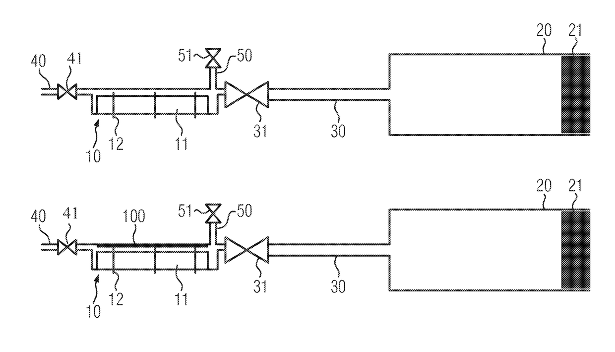
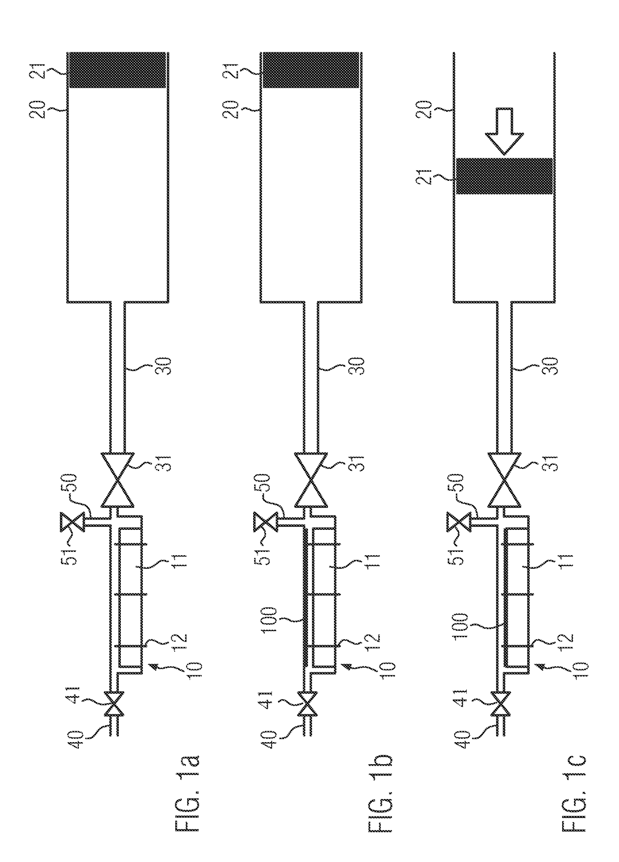
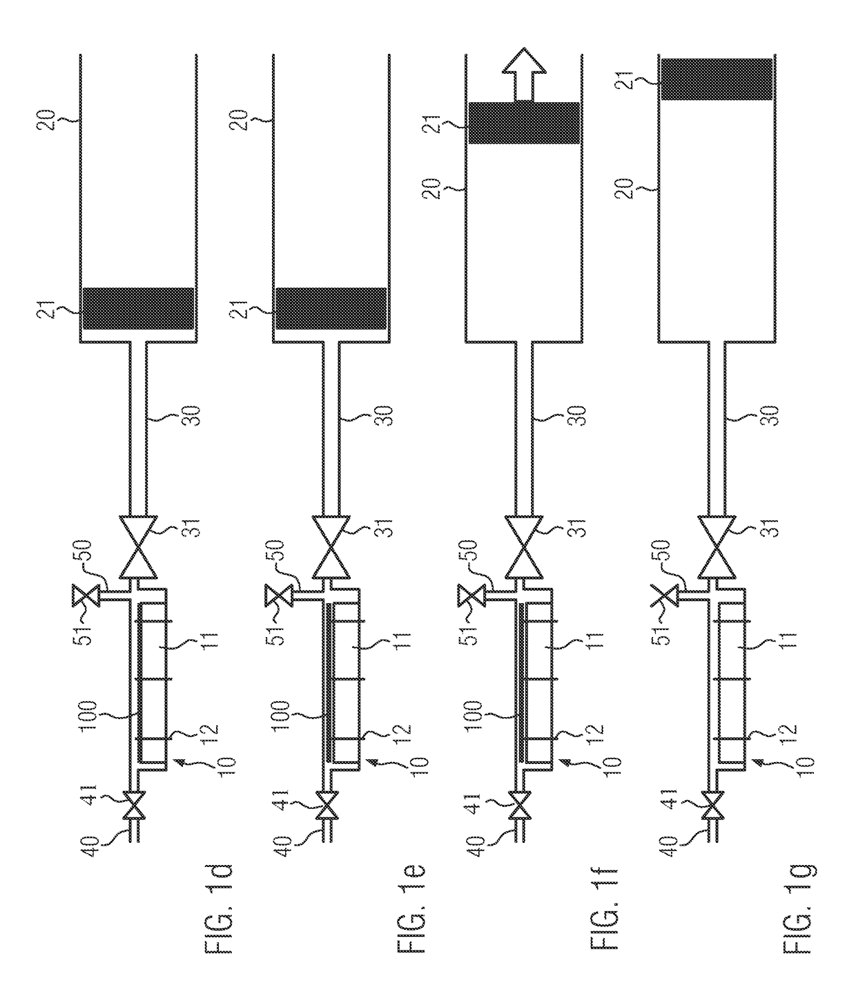
[0020]Various illustrative embodiments of the invention are described below. In the interest of clarity, not all features of an actual implementation are described in this specification. It will of course be appreciated that in the development of any such actual embodiment, numerous implementation-specific decisions must be made to achieve the developers' specific goals, such as compliance with system-related and business-related constraints, which will vary from one implementation to another. Moreover, it will be appreciated that such a development effort might be complex and time-consuming, but would nevertheless be a routine undertaking for those of ordinary skill in the art having the benefit of this disclosure.

[0021]The following embodiments are described in sufficient detail to enable those skilled in the art to make use of the present disclosure. It is to be understood that other embodiments would be evident, based on the present disclosure, and that system, structure, proces...


PUM


Abstract

A method of treating a semiconductor device is provided including the steps of loading the semiconductor device in a processing chamber, pressurizing the processing chamber by supplying a processing gas from a pressure chamber to the processing chamber, performing a thermal anneal of the semiconductor device in the processing chamber, and depressurizing the processing chamber by supplying the processing gas from the processing chamber to the pressure chamber.

Description

BACKGROUND OF THE INVENTION[0001]1. Field of the Invention[0002]Generally, the present disclosure relates to the field of manufacturing of integrated circuits and semiconductor devices, and, more particularly, to anneal treatment of semiconductor devices.[0003]2. Description of the Related Art[0004]The fabrication of advanced integrated circuits, such as CPUs, storage devices, ASICs (application specific integrated circuits) and the like, requires the formation of a large number of circuit elements on a given chip area according to a specified circuit layout. In a wide variety of electronic circuits, field effect transistors represent one important type of circuit element that substantially determines performance of the integrated circuits. Generally, a plurality of process technologies are currently practiced for forming field effect transistors, wherein, for many types of complex circuitry, MOS technology is currently one of the most promising approaches due to the superior charac...

Claims


Application Information

Patent Timeline
Patent Type & Authority Patents(United States)
IPC IPC(8): H01L21/336H01L29/66H01L21/28H01L21/324H01L23/48H01L21/67F27B17/00
CPCH01L21/324F27B17/0025H01L21/28185H01L21/67098H01L29/66568H01L21/28176H01L21/6719
Inventor PETHE, WIELANDNOACK, DIRKKALLAUCH, BERND
Owner GLOBALFOUNDRIES INC
Why Eureka
Try Eureka