Method for manufacturing OLED device and OLED device manufactured therewith

a manufacturing method and technology for oled devices, applied in the field of display technology, can solve the problems of deterioration of devices, low high manufacturing cost, etc., and achieve the effects of low manufacturing cost, high utilization rate of materials, and low manufacturing method

Active Publication Date: 2017-05-23
TCL CHINA STAR OPTOELECTRONICS TECH CO LTD
View PDF20 Cites 0 Cited by
  • Summary
  • Abstract
  • Description
  • Claims
  • Application Information

AI Technical Summary

Benefits of technology

[0009]An object of the present invention is to provide a method for manufacturing an OLED device and an OLED device manufactured therewith, which has an emissive layer of which each type of sub-pixel is made through solution film casting, wherein at least one type of sub-pixel is made of an organic light-emitting material, where the manufacturing process of the OLED device requires no use of a fine metal mask so that the manufacturing cost is low, the utilization rate of material is high, and the yield rate is good.
[0024]The efficacy of the present invention is that the present invention provides a method for manufacturing an OLED device, wherein each of sub-pixels of an emissive layer is formed through a solution film casting process and an anode, a hole transporting layer, an electron transporting layer, and a cathode are formed through vacuum thermal evaporation processes, so that the method for manufacturing the OLED device requires no use of a fine metal mask thereby making the manufacturing cost incurring with the manufacturing method low, the utilization rate of material high, and the yield rate good; and with at least one sub-pixel of the emissive layer being formed of a quantum dot and at least one sub-pixel being formed of an organic light-emitting material, the manufacturing method according to the present invention, when compared with a manufacturing method where all sub-pixels are formed of quantum dots, has a relatively low manufacturing cost and, when compared with a manufacturing method where all sub-pixels are formed of organic light-emitting materials, provides an OLED device having a better performance. An OLED device manufactured with the present invention combines the advantages of a QD-OLED and a solution-film-cast OLED so as to possesses excellent performance, allowing for application to flat panel displays, televisions, and other fields of displaying.

Problems solved by technology

When a device is in a condition of high brightness or high current density, Joule heat is a major cause for deterioration of the device.
The process is expensive and has a low utilization rate of material and poor yield rate.

Method used


Image

  • Method for manufacturing OLED device and OLED device manufactured therewith
  • Method for manufacturing OLED device and OLED device manufactured therewith
  • Method for manufacturing OLED device and OLED device manufactured therewith

Examples


Embodiment Construction

[0033]To further expound the technical solution adopted in the present invention and the advantages thereof, a detailed description is given to a preferred embodiment of the present invention and the attached drawings.

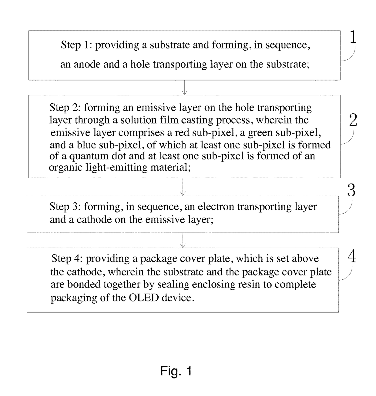
[0034]Referring to FIG. 1, the present invention provides a method for manufacturing an organic light-emitting diode (OLED) device, which comprises:

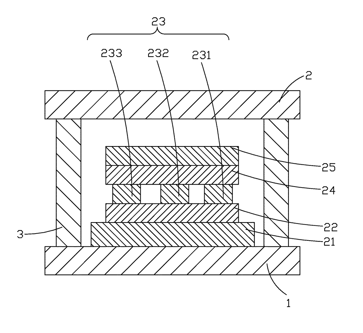
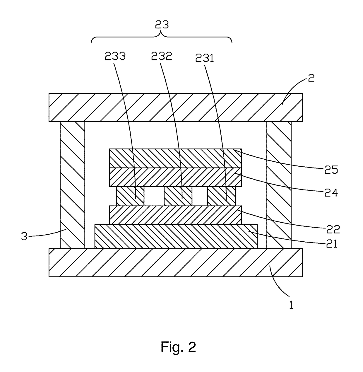
[0035]Step 1: providing a and forming, in sequence, an anode 21 and a hole transporting layer 22 on the substrate 1.

[0036]Step 2: forming an emissive layer 23 on the hole transporting layer 22 through a solution film casting process, wherein the emissive layer 23 comprises a red sub-pixel 231, a green sub-pixel 232, and a blue sub-pixel 233, of which at least one sub-pixel is formed of a quantum dot and at least one sub-pixel is formed of an organic light-emitting material.

[0037]Step 3: forming, in sequence, an electron transporting layer 24 and a cathode 25 on the emissive layer 23.

[0038]Step 4: providing a package cover p...


PUM

PropertyMeasurementUnit
FWHMaaaaaaaaaa
FWHMaaaaaaaaaa
wavelengthaaaaaaaaaa

Abstract

The present invention provides a method for manufacturing an OLED device and an OLED device manufactured therewith. The method for manufacturing an OLED device includes: (1) providing a substrate and forming, in sequence, an anode and a hole transporting layer on the substrate; (2) forming an emissive layer on the hole transporting layer through a solution film casting process, wherein the emissive layer comprises a red sub-pixel, a green sub-pixel, and a blue sub-pixel, of which at least one sub-pixel is formed of a quantum dot and at least one sub-pixel is formed of an organic light-emitting material; (3) forming, in sequence, an electron transporting layer and a cathode on the emissive layer; and (4) providing a package cover plate, which is set above the cathode, wherein the substrate and the package cover plate are bonded together by sealing enclosing resin to complete packaging of the OLED device. Since each sub-pixel of the emissive layer is formed through a solution film casting process, the manufacture of the OLED device requires no use of a fine metal mask so that the manufacturing cost is low, the utilization rate of material is high, and the yield rate is good.

Description

BACKGROUND OF THE INVENTION[0001]1. Field of the Invention[0002]The present invention relates to the field of displaying technology, and in particular to a method for manufacturing an OLED device and an OLED device manufactured therewith.[0003]2. The Related Arts[0004]An OLED (Organic Light-Emitting Diode) is a flat panel displaying technique of extremely prosperous future and it shows excellent displaying performance and also possesses various advantages, such as being self-luminous, simple structure, being ultra-thin, fast response, wide view angle, low power consumption, and being capable of achieving flexible displaying and is thus regarded as a “dream display”. In addition, the investment of manufacturing installation is far less than that of liquid crystal displays so that it has attracted the attention of major display manufacturers and becomes the mainstream of the third-generation display devices of the field of displaying technology.[0005]Semiconductor nanocrystals (NCs) a...

Claims


Application Information

Patent Timeline
Patent Type & Authority Patents(United States)
IPC IPC(8): H01L51/00H01L27/32B82Y20/00H01L51/56H01L51/50H01L51/52B82Y40/00
CPCH01L51/502B82Y20/00H01L27/3211H01L27/3244H01L51/001H01L51/0003H01L51/5056H01L51/5072H01L51/5206H01L51/5221H01L51/5253H01L51/56B82Y40/00H01L51/0035H01L51/0037H01L51/0058H01L51/0061H01L51/0065H01L51/0067H01L51/0072H01L51/0081H01L51/0085H01L51/5012H01L2227/323Y10S977/774Y10S977/824Y10S977/89Y10S977/952H10K71/12H10K71/164H10K50/125H10K71/00H10K59/35H10K50/115H10K50/11H10K50/15H10K50/16H10K50/81H10K50/82H10K50/844H10K59/12H10K59/1201H10K85/111H10K85/324H10K85/342H10K85/626H10K85/636H10K85/653H10K85/654H10K85/1135H10K85/6572
Inventor LIU, YAWEIWANG, YIFAN
Owner TCL CHINA STAR OPTOELECTRONICS TECH CO LTD
Why Eureka
Try Eureka