Manufacturing method of a pixel structure

a manufacturing method and pixel structure technology, applied in the field of display technology, can solve problems such as affecting display quality and inconvenient operation, and achieve the effects of reducing the distance between the pixel electrode, increasing the storage capacitance of the pixel structure, and reducing the influence of a feed-through voltag

Active Publication Date: 2017-06-20
TCL CHINA STAR OPTOELECTRONICS TECH CO LTD
View PDF7 Cites 0 Cited by
  • Summary
  • Abstract
  • Description
  • Claims
  • Application Information

AI Technical Summary

Benefits of technology

[0010]Thus, an object of the present invention is to provide a pixel structure, which decreases the distance between a pixel electrode and a common electrode to increase the storage capacitance of the pixel structure, so as to reduce the influence of a feed-through voltage and electrical leakage on displaying quality of an FFS LCD using such a pixel structure.
[0011]Another object of the present invention is to provide a manufacturing method of a pixel structure, which manufacturing method is simple and applies a second time etching to increase the storage capacitance of the pixel structure so as to reduce the influence of a feed-through voltage and electrical leakage on displaying quality of an FFS LCD using such a pixel structure.
[0012]A further object of the present invention is to provide a manufacturing method of a pixel structure, which manufacturing method is simple and provides a passivation layer of a two-layered structure to increase the storage capacitance of the pixel structure so as to reduce the influence of a feed-through voltage and electrical leakage on displaying quality of an FFS LCD using such a pixel structure.
[0033]The efficacy of the present invention is that the present invention provides a pixel structure and a manufacturing method thereof, wherein a second time etching operation or a two-layered structure of passivation layer is adopted to reduce the distance between a common electrode and a pixel electrode so as to increase storage capacitance of the pixel structure and at the same time, the distance between a data line and the common electrode is increased to reduce harmful parasitic capacitance so as to reduce the influence of a feed-through voltage and electrical leakage on displaying quality of an FFS liquid crystal display that uses the pixel structure. Further, the manufacturing method of the pixel structure is relatively simple.

Problems solved by technology

This would cause insufficient charging of some pixels of a liquid crystal panel thereby displaying incorrect gray level and affecting displaying quality.

Method used


Image

  • Manufacturing method of a pixel structure
  • Manufacturing method of a pixel structure
  • Manufacturing method of a pixel structure

Examples


Embodiment Construction

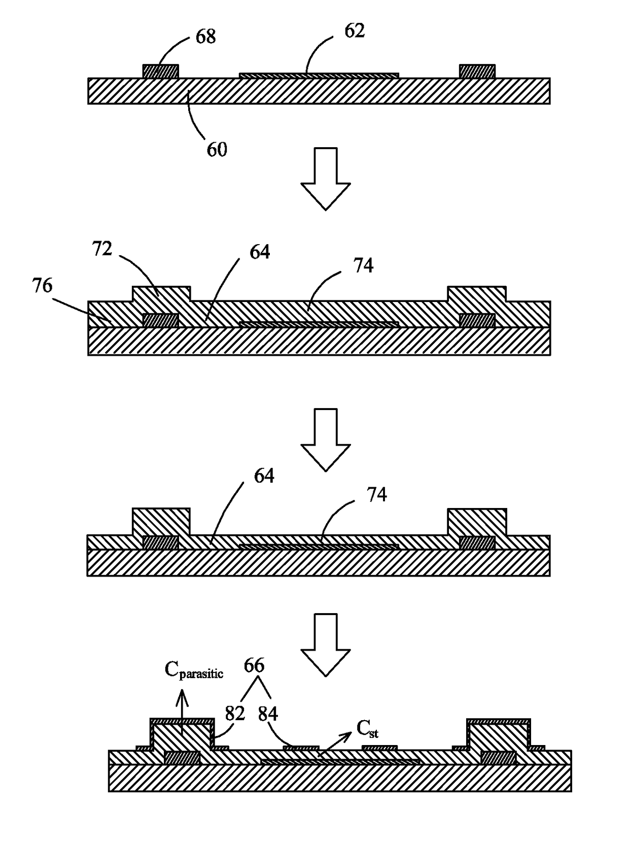
[0044]To further expound the technical solution adopted in the present invention and the advantages thereof, a detailed description is given to a preferred embodiment of the present invention and the attached drawings.

[0045]Referring to FIG. 4, the present invention provides a pixel structure, which comprises:

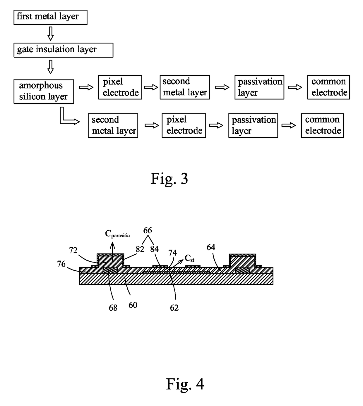
[0046]a transparent substrate 60, a gate line (not shown for the purposes of easy observation) formed on the transparent substrate 60, a thin-film transistor (not shown for the purposes of easy observation) formed on the transparent substrate 60, a data line 68 formed on the transparent substrate 60, a pixel electrode 62 formed on the transparent substrate 60 and the thin-film transistor, a passivation layer 64 formed on the pixel electrode 62, the transparent substrate 60, and the data line 68, and a common electrode 66 formed on the passivation layer 64.

[0047]The passivation layer 64 comprises: a first portion 72 located on the data line 68, a second portion 74 located on the...


PUM

PropertyMeasurementUnit
thicknessaaaaaaaaaa
transparentaaaaaaaaaa
thicknessaaaaaaaaaa

Abstract

The present invention provides a pixel structure and a manufacturing method thereof. The pixel structure includes: a transparent substrate (60), a gate line formed on the transparent substrate (60), a thin-film transistor formed on the transparent substrate (60), a data line (68) formed on the transparent substrate (60), a pixel electrode (62) formed on the transparent substrate (60) and the thin-film transistor, a passivation layer (64) formed on the pixel electrode (62), the transparent substrate (60), and the data line (68), and a common electrode (66) formed on the passivation layer (64). The passivation layer (64) includes: a first portion (72) located on the data line (68), a second portion (74) located on the pixel electrode (62), and a third portion (76) located on the transparent substrate (60) and arranged on two opposite sides of the data line (68). The first portion (72) of the passivation layer (64) has a thickness greater than a thickness of the second portion (74).

Description

BACKGROUND OF THE INVENTION[0001]1. Field of the Invention[0002]The present invention relates to the field of displaying technology, and in particular to a pixel structure and a manufacturing method thereof.[0003]2. The Related Arts[0004]The displaying technology has undergone rapid progress recently. A flat display device applies totally different techniques of displaying and manufacturing, making it significantly differing from the conventional video image displaying devices. The conventional video image displaying device is generally based on a cathode ray tube (CRT), from which a flat display device is made different primarily concerning changes made in respect of weight and size (thickness). Generally, a flat display device has a thickness not greater than 10 centimeters, among the other differences associated with various technical aspects, such as theory of displaying, manufacturing material, manufacturing process, driving for displaying video images.[0005]A liquid crystal di...

Claims


Application Information

Patent Timeline
Patent Type & Authority Patents(United States)
IPC IPC(8): H01L27/12G02F1/1343
CPCH01L27/1255G02F1/134309H01L27/124H01L27/1262G02F2001/134372G02F1/134372G02F1/1343G02F1/1368
Inventor HAO, SIKUN
Owner TCL CHINA STAR OPTOELECTRONICS TECH CO LTD
Why Eureka
Try Eureka