Variable capacitance device

a variable capacitance and capacitance element technology, applied in the direction of thin/thick film capacitors, fluid speed measurement, instruments, etc., can solve the problems of poor resistance property of esd (electro-static discharge) and deterioration of esd resistance properties, and reduce control sensitivity. , the reliability of the variable capacitance element section may be increased, and the number of elements may be significantly reduced.

Active Publication Date: 2017-07-11
MURATA MFG CO LTD
View PDF25 Cites 8 Cited by
  • Summary
  • Abstract
  • Description
  • Claims
  • Application Information

AI Technical Summary

Benefits of technology

[0010]According to the structure described above, the variable capacitance element section is formed in the redistribution layer, and the ESD protection element is formed in the semiconductor substrate. Accordingly, isolation between the variable capacitance element section and the ESD protection element section may be easily secured, and a small variable capacitance device with high ESD resistance and high control sensitivity may be configured.
[0012]Preferably, in plan view, the variable capacitance element section is provided at a position not overlapping the ESD protection element and the electrode pad for the ESD protection element. This allows isolation between the variable capacitance element section and the ESD protection element section to be more easily secured, and also, allows flatness of the underlying portion of the variable capacitance element section to be secured, and the reliability of the variable capacitance element section may be increased.
[0013]Preferably, a resistance element is provided between the variable capacitance element section and a control voltage application terminal, and the resistance element is formed on a layer, in the redistribution layer, where the variable capacitance element section is provided, opposite the semiconductor substrate. This eliminates the need to provide a resistance element outside, and the number of elements may be significantly reduced. Also, because the resistance element is formed on a layer where the variable capacitance element section is provided, opposite the semiconductor substrate, flatness of the variable capacitance element section is not negatively affected, and also, isolation between the ESD protection element section and the resistance element may be increased.
[0014]Preferably, an insulating layer is provided between the variable capacitance element section and the semiconductor substrate. That is, by forming an insulating layer between the semiconductor substrate and the capacitor electrode, isolation between the ESD protection section and the variable capacitance element section may be further increased.
[0015]Accordingly, the present disclosure provides a small ESD-resistant variable capacitance device with high control sensitivity may be achieved.

Problems solved by technology

A variable capacitance element including a ferroelectric film has a disadvantage in that that an ESD (Electro-Static Discharge) resistance property is poor compared to an MEMS variable capacitance element or a variable capacitance element of a semiconductor, such as a variable capacitance diode.
Moreover, when the thickness of the ferroelectric film is reduced is certain designs, the control sensitivity (the ratio of a change in the capacitance value to a change in the control voltage) will be increased, but the ESD resistance property will deteriorate due to the reduction in the thickness of the ferroelectric film.
Accordingly, there is a restriction in reducing the thickness of the ferroelectric film from the standpoint of the ESD resistance, and the control sensitivity is also restricted.

Method used


Image

  • Variable capacitance device
  • Variable capacitance device
  • Variable capacitance device

Examples


first embodiment

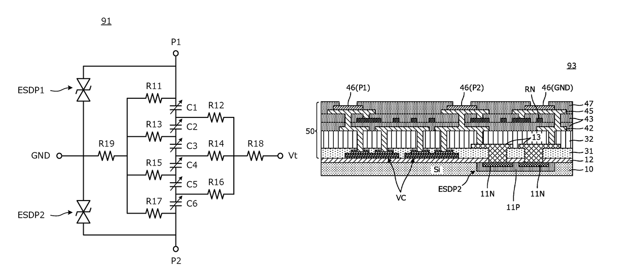
[0031]FIG. 1 is a circuit diagram of a variable capacitance device 91 according to a first embodiment. The variable capacitance device 91 includes variable capacitance elements C1 to C6, RF resistance elements R11 to R19, and ESD protection elements ESDP1, ESDP2.

[0032]A capacitance value of the variable capacitance elements C1 to C6 is determined based on a control voltage applied between a control voltage input terminal Vt and a ground terminal GND, and a capacitance value between a first input / output terminal P1 and a second input / output terminal P2 is thereby determined.

[0033]Each of the variable capacitance elements C1 to C6 is a ferroelectric capacitor formed from a ferroelectric film whose dielectric constant is changed by an electric field, and capacitor electrodes sandwiching the ferroelectric film to apply voltage thereto. The dielectric constant of the ferroelectric film changes due to the amount of polarization being changed according to the intensity of an applied electr...

second embodiment

[0055]FIGS. 5A and 5B show cross-sectional views showing structures and a manufacturing method of a variable capacitance device 92 according to a second embodiment. The circuit diagram is the same as the one shown in FIG. 1 for the first embodiment.

[0056]In the following, the structure and the manufacturing method of the variable capacitance device according to the present embodiment will be described in order with reference to FIGS. 5A and 5B. As shown, FIGS. 5A and 5B will be described in the order of manufacturing, including steps (1) through (5) shown in FIG. 3A and steps (6) through (7) shown in FIG. 5B. One or more of these steps may contain sub-steps as described below.

[0057]In step (1), an SiO2 film 12 is formed on an N-type Si substrate 10, and active regions 11 are formed at regions where ESD protection elements are to be formed, by impurity diffusion by ion implantation or the like.

[0058]In step (2), BST films and Pt electrode films are alternately laminated on the SiO2 f...

third embodiment

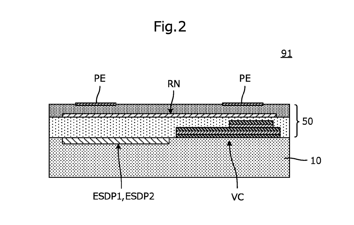
[0067]FIG. 7 is a cross-sectional view of a variable capacitance device 93 according to a third embodiment. As shown, the variable capacitance device 93 includes variable capacitance element sections VC, resistance element sections RN, an ESD protection element ESDP2, and the like.

[0068]FIGS. 8A to 8E are cross-sectional views showing structures and a manufacturing method of the variable capacitance device 93.

[0069]In the following, the structure and the manufacturing method of the variable capacitance device according to the present embodiment will be described in order with reference to FIGS. 8A to 8E, including manufacturing steps (1) through (19), respectively. Moreover, one or more of these steps may contain sub-steps as described below.

[0070]In step (1), an N-type Si substrate 10 is prepared.

[0071]In step (2), an SiO2 film 12P is formed on the N-type Si substrate 10, and active regions 11P, 11N are formed at regions where an ESD protection element of the Si substrate 10 is for...


PUM


Abstract

A variable capacitance device that includes a semiconductor substrate, a redistribution layer disposed on a surface of the semiconductor substrate, and a plurality of terminal electrodes including first and second input / output terminals, a ground terminal and a control voltage application terminal. Moreover, a variable capacitance element section is formed in the redistribution layer from a pair of capacitor electrodes connected to the first and second input / output terminals, respectively, and a ferroelectric thin film disposed between the capacitor electrodes. Further, an ESD protection element is connected between the one of the input / output terminals and the ground terminal is formed on the surface of the semiconductor substrate.

Description

CROSS REFERENCE TO RELATED APPLICATIONS[0001]The present application is a continuation of PCT / JP2015 / 057814 filed Mar. 17, 2015, which claims priority to Japanese Patent Application No. 2014-077102, filed Apr. 3, 2014, the entire contents of each of which are incorporated herein by reference.TECHNICAL FIELD[0002]The present disclosure relates to a variable capacitance device used for a communication device for a Radio Frequency Identification (RFID) system or a Near Field Communication (NFC) system, for example.BACKGROUND[0003]Conventionally, variable capacitance elements whose dielectric constant is changed by a control voltage are proposed by Patent Literatures 1 and 2, for example. These variable capacitance elements adopt a laminated structure (i.e., an MIM structure) of a metal, a ferroelectric material, and a metal, and are provided with a ferroelectric thin film so that a large amount of change in the capacitance may be achieved by low voltage.[0004]Patent Literature 1: JP 45...

Claims


Application Information

Patent Timeline
Patent Type & Authority Patents(United States)
IPC IPC(8): H01L27/02H01L27/08B81B7/00H01G7/06H01L29/93H01L49/02
CPCH01L27/0248B81B7/0022H01G7/06H01L27/0805H01L29/93B81B2201/0221H01L28/55H01G4/33
Inventor NAKAISO, TOSHIYUKISAKAI, NOBUO
Owner MURATA MFG CO LTD
Why Eureka
Try Eureka