Dual function hybrid memory cell

a memory cell and hybrid technology, applied in the field of memory and storage devices, can solve the problems of nvm memory devices being more expensive but less power, information stored in dram will eventually degrade, and consuming large amounts of power, so as to reduce write voltage, shorten data retention time, and reduce write voltage

Active Publication Date: 2017-07-25
NEO SEMICON
View PDF12 Cites 2 Cited by
  • Summary
  • Abstract
  • Description
  • Claims
  • Application Information

AI Technical Summary

Benefits of technology

[0007]In various exemplary embodiments, a novel dual function hybrid memory cell is disclosed. The dual function hybrid memory cell includes two charge-trapping layers between the gate and the channel of the cell. The bottom charge-trapping layer is directly formed on top of the silicon or polysilicon channel. This allows electric charges to be stored in the bottom charge-trapping layer in a much shorter write time and using a lower write voltage. The top charge-trapping layer is isolated by dielectric layers and thus provides much longer data retention. As a result, the single cell may be used as a dual-function memory cell, e.g., DRAM (Dynamic Random-Access Memory) and NVM (Non-Volatile Memory). In one embodiment, the charge-trapping layers and dielectric layers are formed by nitride and oxide layers. Thus, the cell is referred to as a Silicon-Oxide-Nitride-Oxide-Nitride-Silicon (SONONS) cell according to the materials of its vertical structure. In addition to the novel cell structure, several novel programming bias conditions are disclosed that allow either or both of the top and bottom charge-trapping layers to be programmed.

Problems solved by technology

Unfortunately, due to the dynamic nature of its configuration, the information stored in DRAM will eventually degrade unless periodic memory refresh cycles are performed.
Thus, though DRAM memory cells may be small in size, they may also consume large amounts of power due to the refresh requirements.
In contrast to DRAM, NVM memory devices maybe more expensive but consumes less power.
For example, utilizing DRAM memory for speed and NVM memory for data retention may increase the overall space and size requirements of the system.

Method used


Image

  • Dual function hybrid memory cell
  • Dual function hybrid memory cell
  • Dual function hybrid memory cell

Examples


Embodiment Construction

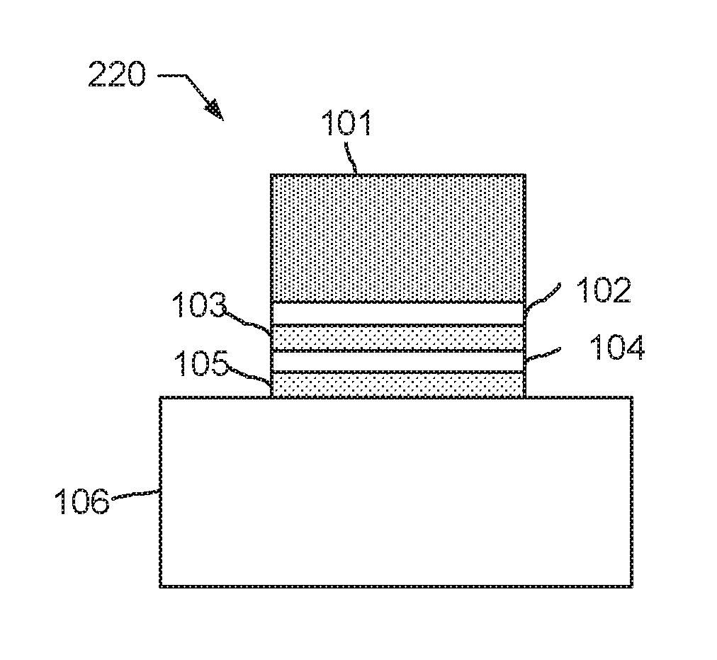
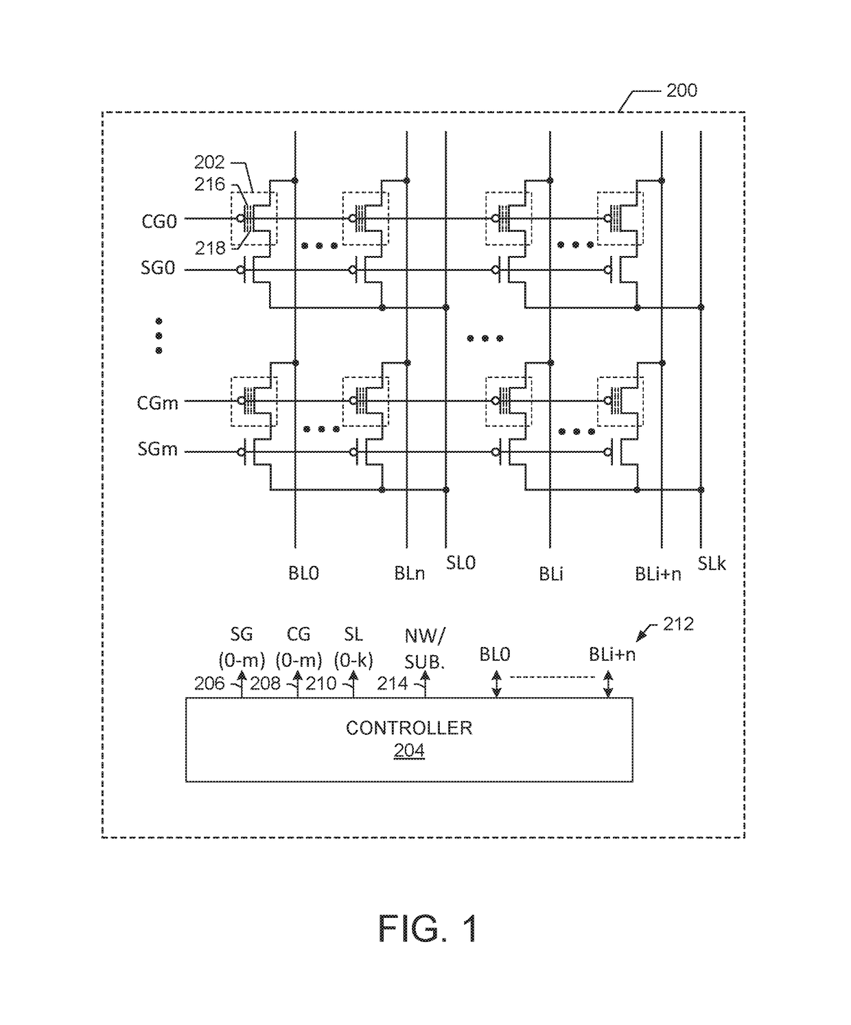
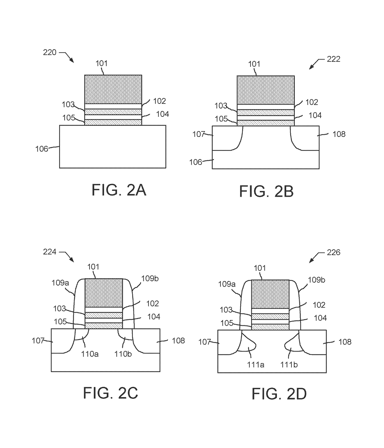
[0022]Exemplary embodiments of the present invention are described herein in the context of a process, device, method, and apparatus for providing a novel dual function hybrid memory cell.

[0023]Those of ordinary skilled in the art will realize that the following detailed description is illustrative only and is not intended to be in any way limiting. Other embodiments of the present invention will readily suggest themselves to skilled persons having the benefit of this disclosure. Reference will now be made in detail to implementations of the exemplary embodiments of the present invention as illustrated in the accompanying drawings. The same reference indicators (or numbers) will be used throughout the drawings and the following detailed description to refer to the same or like parts.

[0024]It should be noted that the exemplary embodiments are not limited to SONONS cells only and the disclosed aspects can be applied to other types of charge-trapping cells. To realize the low-cost, hig...


PUM


Abstract

A dual function hybrid memory cell is disclosed. In one aspect, the memory cell includes a substrate, a bottom charge-trapping region formed on the substrate, a top charge-trapping region formed on the bottom charge-trapping region, and a gate layer formed on the top charge trapping region. In another aspect, a method for programming a memory cell having a substrate, a bottom charge-trapping layer, a top charge-trapping layer, and a gate layer is disclosed. The method includes biasing a channel region of the substrate, applying a first voltage differential between the gate layer and the channel region, injecting charge into the bottom charge-trapping layer from the channel region based on the first voltage differential. The method also includes applying a second voltage differential between the gate layer and the channel region and injecting charge from the bottom charge-trapping layer into the top charge-trapping layer based on the second voltage differential.

Description

PRIORITY[0001]This application claims the benefit of priority based upon U.S. Provisional Patent Application having Application No. 62 / 152,813, filed on Apr. 24, 2015, and entitled “SONONS—DRAM and NVM Dual-Function Hybrid Memory,” which is hereby incorporated herein by reference in its entirety.FIELD OF THE INVENTION[0002]The exemplary embodiments of the present invention relate generally to the field of semiconductors and integrated circuits, and more specifically to memory and storage devices.BACKGROUND OF THE INVENTION[0003]Memory devices are widely used in a variety of digital electronics. One type of memory device is a dynamic random access memory (DRAM) device. DRAM devices can be used to form low cost high density memory arrays. For example, one of the largest applications for DRAM is as the main memory in modern computers. Unfortunately, due to the dynamic nature of its configuration, the information stored in DRAM will eventually degrade unless periodic memory refresh cycl...

Claims


Application Information

Patent Timeline
Patent Type & Authority Patents(United States)
IPC IPC(8): G11C16/04H01L27/12G11C11/401H01L29/423H01L29/66H01L29/78G11C7/10H01L29/792G11C16/10H01L21/28
CPCG11C16/0475G11C7/1015G11C11/401G11C16/10H01L21/28282H01L27/1211H01L29/4234H01L29/66833H01L29/785H01L29/792G11C16/0466G11C2211/4016H01L29/40117
Inventor HSU, FU-CHANG
Owner NEO SEMICON
Why Eureka
Try Eureka