RRAM device and method for manufacturing the same

a random access memory and rram technology, applied in the direction of bulk negative resistance effect devices, semiconductor devices, electrical equipment, etc., can solve the problem of ineffective rram devices

Active Publication Date: 2017-07-25
WINBOND ELECTRONICS CORP
View PDF6 Cites 9 Cited by
  • Summary
  • Abstract
  • Description
  • Claims
  • Application Information

AI Technical Summary

Problems solved by technology

However, the oxygen atoms may diffuse back to the resistive switching layer o

Method used


Image

  • RRAM device and method for manufacturing the same
  • RRAM device and method for manufacturing the same
  • RRAM device and method for manufacturing the same

Examples


Embodiment Construction

[0022]The following description is of the best-contemplated mode of carrying out the invention. This description is made for the purpose of illustrating the general principles of the invention and should not be taken in a limiting sense. The scope of the invention is best determined by reference to the appended claims.

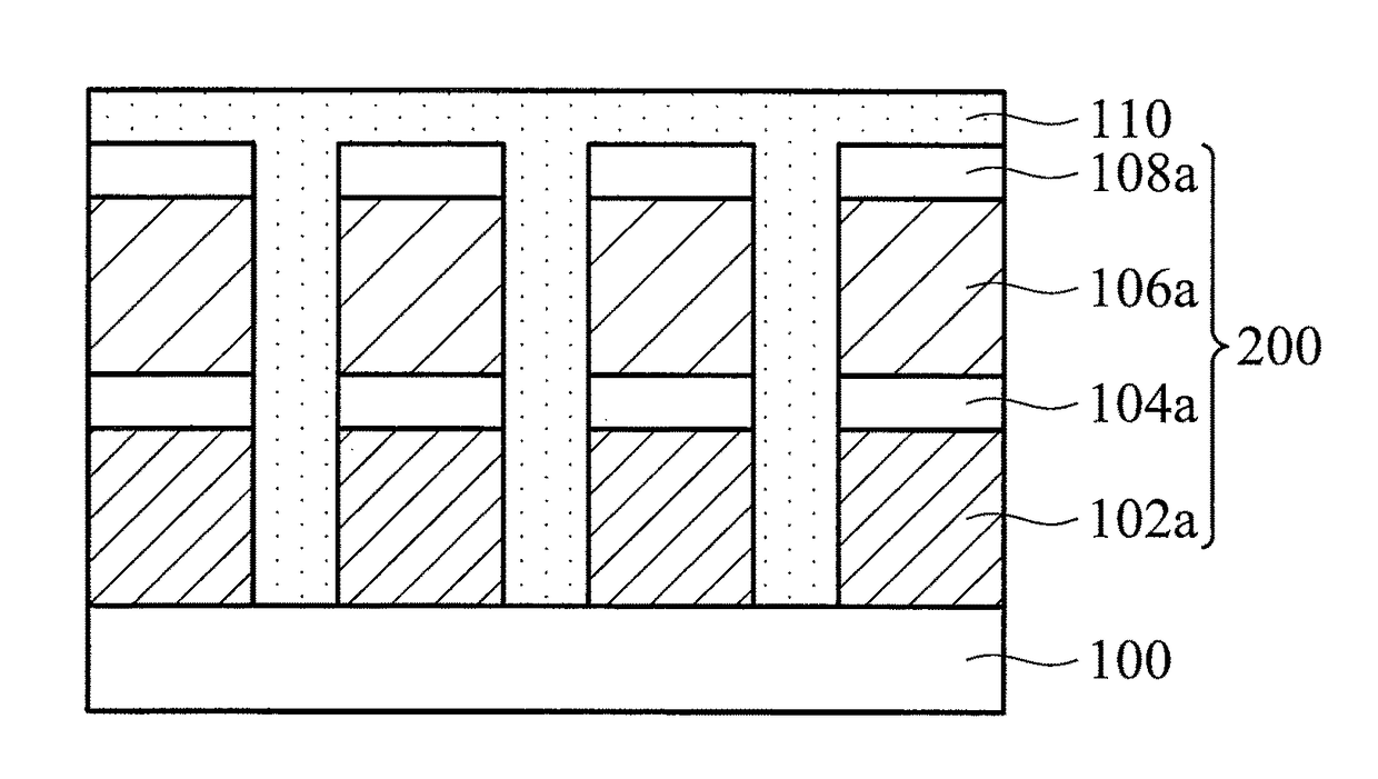
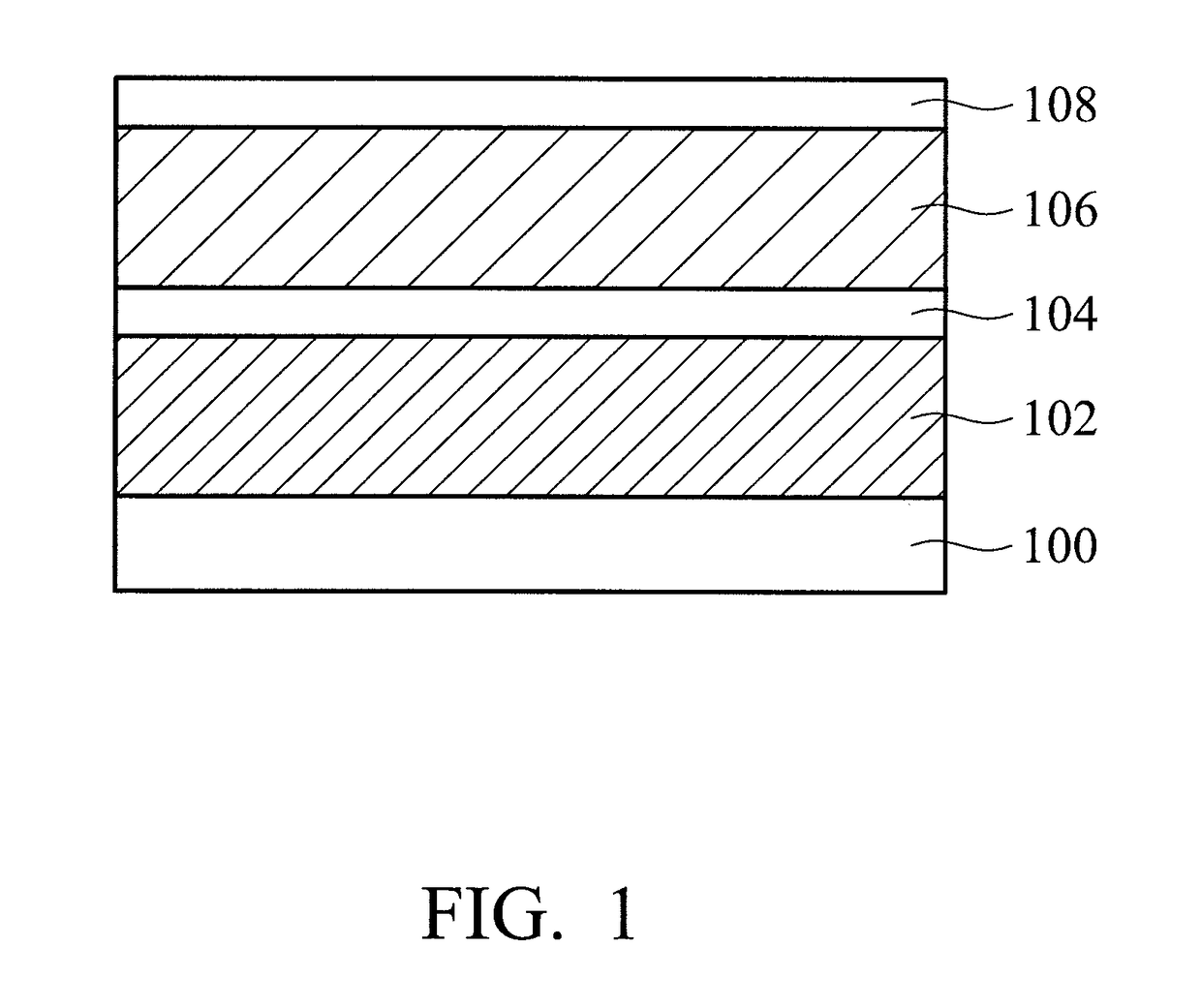
[0023]FIGS. 1, 3-5 are schematic cross sections showing a method for forming an exemplary resistive random access memory (RRAM) device.

[0024]In FIG. 1, a semiconductor structure (not shown) with a bottom electrode 100 formed over the semiconductor structure is provided. The semiconductor structure comprises at least a semiconductor substrate (not shown) such as a silicon wafer and a memory controlling element (not shown) such as an active controlling element (e.g. a transistor) or a passive controlling element (e.g. a conductive line) formed over the semiconductor substrate. At this time, the bottom electrode 100 may be a patterned conductive layer formed in a portion ...


PUM


Abstract

A resistive random access memory device includes a bottom electrode, a plurality of memory stacks separately formed over the bottom electrode, a third oxygen diffusion barrier layer formed between the memory stacks, and a top electrode formed over the plurality of memory stacks and the third oxygen diffusion barrier layer. Each of the plurality of memory stacks includes a resistive switching layer formed over the bottom electrode, a first oxygen diffusion barrier layer formed over the resistive switching layer, a conductive oxygen reservoir layer formed over the first oxygen diffusion barrier layer, and a second oxygen diffusion barrier layer formed over the conductive oxygen reservoir layer.

Description

BACKGROUND OF THE INVENTION[0001]Field of the Invention[0002]The disclosure relates to a resistive random access memory (RRAM) device, and in particular it relates to a resistive random access memory (RRAM) device having a plurality of patterned memory stacks, and a method for manufacturing the same.[0003]Description of the Related Art[0004]The resistive random access memory (RRAM) device has become a major stream of the newly developed non-volatile memory due to the following advantages: low power consumption, low operation voltage, short write and erase times, long endurance, long data retention time, non-destructive read operation, multi-state memory, being simple to manufacture, and having scalable properties. The basic structure of the RRAM device includes a metal-insulator-metal (MIM) stack of a bottom electrode, a resistive switching layer, and a top electrode. The resistive switching (RS) property is an important property of the RRAM device. For example, when a writing volta...

Claims


Application Information

Patent Timeline
IPC IPC(8): H01L47/00H01L45/00H01L27/24
CPCH01L45/1246H01L45/085H01L45/1233H01L45/1266H01L45/146H01L45/1625H01L27/2463H10B63/30H10N70/24H10N70/826H10N70/8833H10N70/063
Inventor CHEN, FREDERICK
Owner WINBOND ELECTRONICS CORP
Why Eureka
Try Eureka