Photoelectric device and electronic apparatus including the same

a technology of photoelectric devices and electronic devices, applied in electrical devices, semiconductor devices, radio frequency controlled devices, etc., can solve the problems of image blur, reduced size of photoelectric devices in pixels, etc., and achieve excellent photoelectric conversion characteristics and carrier (charge) transfer characteristics

Active Publication Date: 2017-11-07
SAMSUNG ELECTRONICS CO LTD
View PDF37 Cites 6 Cited by
  • Summary
  • Abstract
  • Description
  • Claims
  • Application Information

AI Technical Summary

Benefits of technology

[0007]One or more exemplary embodiments may provide are photoelectric devices that may actively determine a wavelength band of an absorbed (detected) light. One or more exemplary embodiments may provide photoelectric devices that have excellent photoelectric conversion characteristics and carrier (charge) transfer characteristics.
[0008]One or more exemplary embodiments may provide photoelectric devices that have a high responsivity and a high detectivity. One or more exemplary embodiments may provide photoelectric devices that have a high optical gain and a high sensitivity. One or more exemplary embodiments may provide photoelectric devices that may be easily capable of high integration and high resolution.
[0009]One or more exemplary embodiments may provide photoelectric devices that may realize an RGB pixel without a color filter. One or more exemplary embodiments may provide photoelectric devices wherein a pixel size in a horizontal direction may be greatly reduced by stacking subpixels in a vertical direction.

Problems solved by technology

However, when color filters are used, image blur may occur due to light crossover or light scattering.
Also, when the degree of integration and resolution of a device increase, the size of a photoelectric device in a pixel is reduced, and various limits and problems may be caused, such as fill factor reduction and optical gain reduction.

Method used


Image

  • Photoelectric device and electronic apparatus including the same
  • Photoelectric device and electronic apparatus including the same
  • Photoelectric device and electronic apparatus including the same

Examples


Embodiment Construction

[0108]Reference will now be made in detail to exemplary embodiments which are illustrated in the accompanying drawings, wherein like reference numerals refer to like elements throughout. In this regard, the present exemplary embodiments may have different forms and should not be construed as being limited to the descriptions set forth herein. Accordingly, the exemplary embodiments are merely described below, by referring to the figures, to explain certain aspects of the embodiments. As used herein, the term “and / or” includes any and all combinations of one or more of the associated listed items. Expressions such as “at least one of,” when preceding a list of elements, modify the entire list of elements and do not modify the individual elements of the list.

[0109]Various exemplary embodiments will now be described more fully with reference to the accompanying drawings.

[0110]It will be understood that when an element is referred to as being “connected” or “coupled” to another element, ...


PUM


Abstract

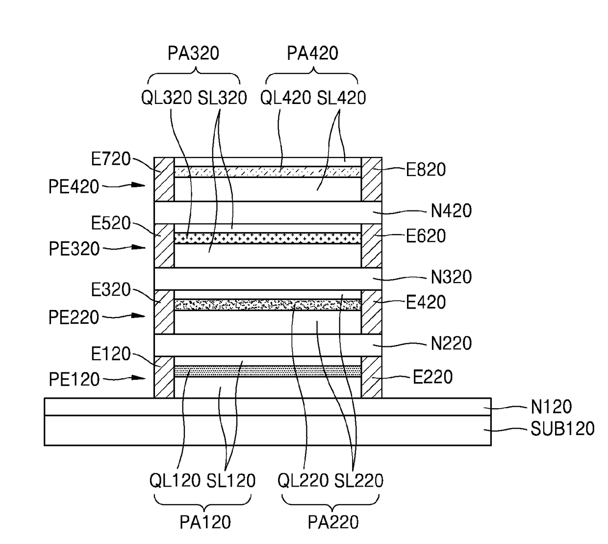
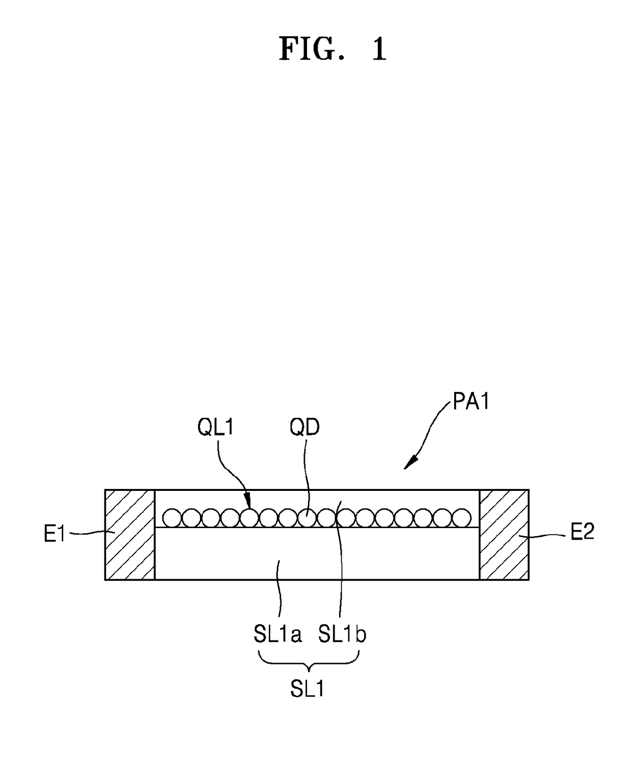
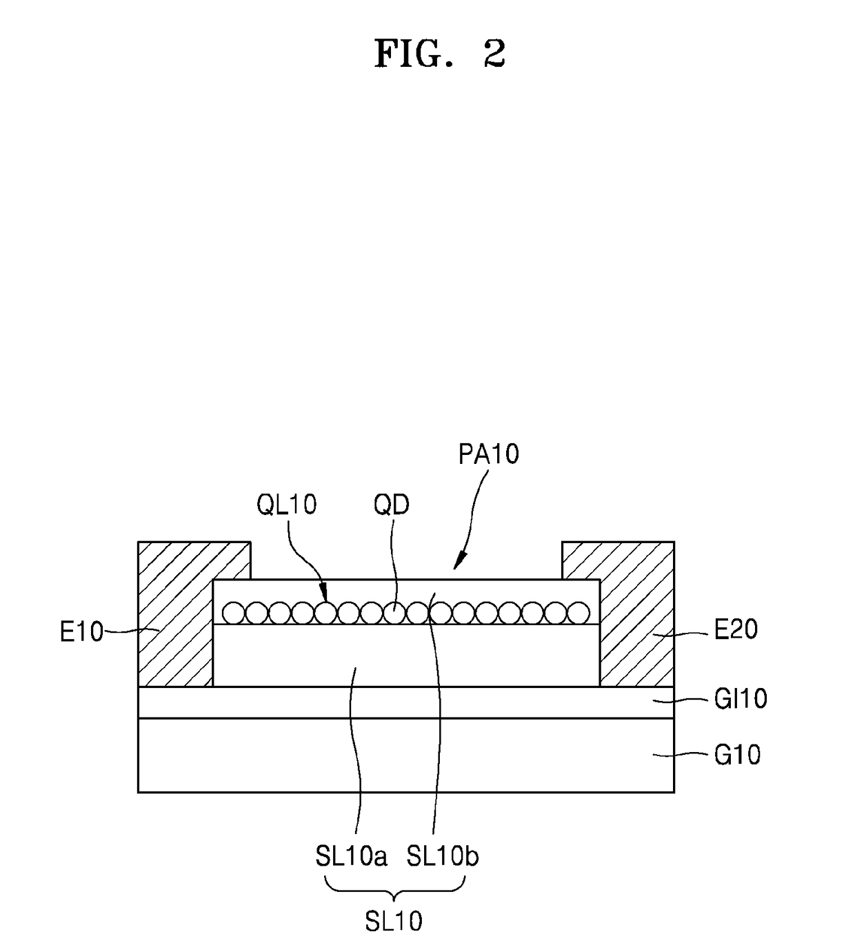
Provided are photoelectric devices and electronic apparatuses including the photoelectric devices. A photoelectric device may include a photoactive layer, the photoactive layer may include a nanostructure layer configured to generate a charge in response to light and a semiconductor layer adjacent to the nanostructure layer. The nanostructure layer may include one or more quantum dots. The semiconductor layer may include an oxide semiconductor. The photoelectric device may include a first electrode and a second electrode that contact different regions of the photoactive layer. A number of the photoelectric conversion elements may be arranged in a horizontal direction or may be stacked in a vertical direction. The photoelectric conversion elements may absorb and thereby detect light in different wavelength bands without the use of color filters.

Description

CROSS-REFERENCE TO RELATED APPLICATION[0001]This application claims priority from Korean Patent Application No. 10-2015-0131892, filed on Sep. 17, 2015, in the Korean Intellectual Property Office, the disclosure of which is incorporated herein in its entirety by reference.BACKGROUND[0002]1. Field[0003]Apparatuses consistent with exemplary embodiments relate to photoelectric devices and electronic apparatuses including the same.[0004]2. Description of the Related Art[0005]Photoelectric devices convert optical energy into electrical energy and generate electrical signals or power in response to light such as visible rays, infrared rays, and ultraviolet rays. Photodiodes and solar cells are examples of photoelectric devices.[0006]Photoelectric devices may be utilized in image sensors, photosensors, or the like. Red, green, and blue (RGB) pixels may be used in complementary metal-oxide semiconductor (CMOS) image sensors, RGB photosensors, or the like. Typically, a color filter correspon...

Claims


Application Information

Patent Timeline
Patent Type & Authority Patents(United States)
IPC IPC(8): H01L31/0232H01L31/12H01L27/146H01L31/112H01L31/0352H01L31/032B82Y20/00
CPCH01L31/02322H01L27/14647H01L31/032H01L31/1126H01L31/035218Y10S977/954B82Y20/00Y10S977/774H01L27/14645H01L31/1136
Inventor CHO, KYUNGSANGBAIK, CHANWOOKJEONG, HEEJEONG
Owner SAMSUNG ELECTRONICS CO LTD
Why Eureka
Try Eureka