Capacitor enhanced multi-element photovoltaic cell

a photovoltaic cell, multi-element technology, applied in the field of photovoltaic cells, can solve the problems of 7% power loss, blackbody radiation loss, band gap limitations, etc., and achieve the effect of optimizing the energy extraction of the photovoltaic array

Inactive Publication Date: 2017-11-07
BLACK NIGHT ENTERPRISES
View PDF46 Cites 0 Cited by
  • Summary
  • Abstract
  • Description
  • Claims
  • Application Information

AI Technical Summary

Benefits of technology

[0021]The multi-element photovoltaic cell of the present invention may have two or more photovoltaic elements with an isolation layer interposed between all contiguous photovoltaic elements. Also, regardless of the number of photovoltaic elements, each photovoltaic element will have an element front conductor and an element rear conductor which are in electrical contact with the photovoltaic layer of the photovoltaic element. There may also be an anti-reflective coating at the element front of each photovoltaic element. A rear insulation layer may electronically isolate the multi-element photovoltaic cell from its environment.
[0031]The output circuit provides for each photovoltaic element to be connected in series or parallel. For a preferred embodiment, the capacitor switches may be operated by the photovoltaic controller to provide for each group of photovoltaic element capacitors that are to be discharged in series, to be first connected in parallel to provide for equalization of the voltage on each capacitor. This prevents the lowest voltage capacitor in the series from limiting the current when the capacitors are switched to discharging in series.
[0033]It is anticipated, based upon current technology, that the capacitors, switches, voltage sensors, and circuit connections between these components, will be components of an integrated circuit in which the photovoltaic cells are imbedded. The utilization of additional capacitors, switches and voltage sensors for embodiments with a larger number of capacitors for each photovoltaic cell, would certainly increase the cost of the photovoltaic controller of the present invention.
[0035]For a preferred embodiment, the photovoltaic controller may incorporate a digital computer and may communicate by wire or wireless with the capacitor voltage sensors to receive voltage measurements and may communicate by wire or wireless with the charge switches and the discharge switches to cause the switches to open and close as needed to manage the charging and discharging of the photovoltaic element capacitors so as to optimize the energy extraction of the photovoltaic array and to control the voltage and other characteristics of the output from the photovoltaic array so as to appropriately interface with storage, electric grid or other application for the extracted solar energy. For a preferred embodiment, the capacitor switches may be operated by the photovoltaic controller to provide for each group of photovoltaic element capacitors that are to be discharged in series, to be first connected in parallel to provide for equalization of the voltage on each capacitor. This prevents the lowest voltage capacitor in the series from limiting the current when the capacitors are switched to discharging in series.

Problems solved by technology

This limit is based on several loss mechanisms that are inherent to any solar cell.
One type of loss is the blackbody radiation loss which accounts for about 7% of the power loss.
A third and principal loss mechanism results from bandgap limitations, i.e. result from the fact that a photon must have enough energy to exceed the bandgap energy of the material, or it will not excite an electron from its orbit.
Bandgap limitations are a major problem for single layer, single junction solar cells.
This relaxation energy loss is in the form of heat in the cell which may further increase blackbody losses.
Other design concerns, such as reflection off the front surface or the metal terminals, further reduce efficiency.
The higher the number of layers, the higher the theoretical efficiency limit of the cell.
Multi-junction cells are difficult to produce because of the thinness of the materials and the difficulties with extracting the current between the layers.
A monolithically integrated cell having multiple layers that are mechanically and electrically connected, is difficult to produce.
The multiplier on the solar radiation concentration provided by the concentrator lens, particularly if the lens is equipped with solar tracking, may offset the cost / efficiency disadvantage of the multi-junction photovoltaic cells.
The difficulty in matching the photocurrent produced by each layer of a multi-layer photovoltaic cell is further complicated by the variations in the power distribution over the overall operating spectrum range, the “overall bandgap,” for which energy is intended to be absorbed by the photovoltaic cell.
Even variations in atmospheric pressure and humidity may significantly affect the power distribution over the overall bandgap.
Photovoltaic layer material selection and layer design for a sea level, equatorial, frequent cloud cover, and high humidity application, may be poorly suited for a high latitude, high altitude, clear sky, and low humidity application.
Further, a photovoltaic cell with material and layer design selected to optimize efficiency during a particular season, may result in a substantially reduced efficiency during other seasons, when the power distribution within the overall bandgap will be substantially different.
Still further, a photovoltaic cell which has its layer material and layer design selections made based upon a particular time of day, i.e. optimized based upon the power distribution within the overall bandgap during a particular time of day, for example solar noon, may result in substantially diminished efficiency during other times of day, particularly the early morning and later afternoon hours.
Another inherent problem affecting the efficiency of a photovoltaic cell, or a photovoltaic layer of a multi-layer cell is related to the output voltage range of the layer.

Method used


Image

  • Capacitor enhanced multi-element photovoltaic cell
  • Capacitor enhanced multi-element photovoltaic cell
  • Capacitor enhanced multi-element photovoltaic cell

Examples


Embodiment Construction

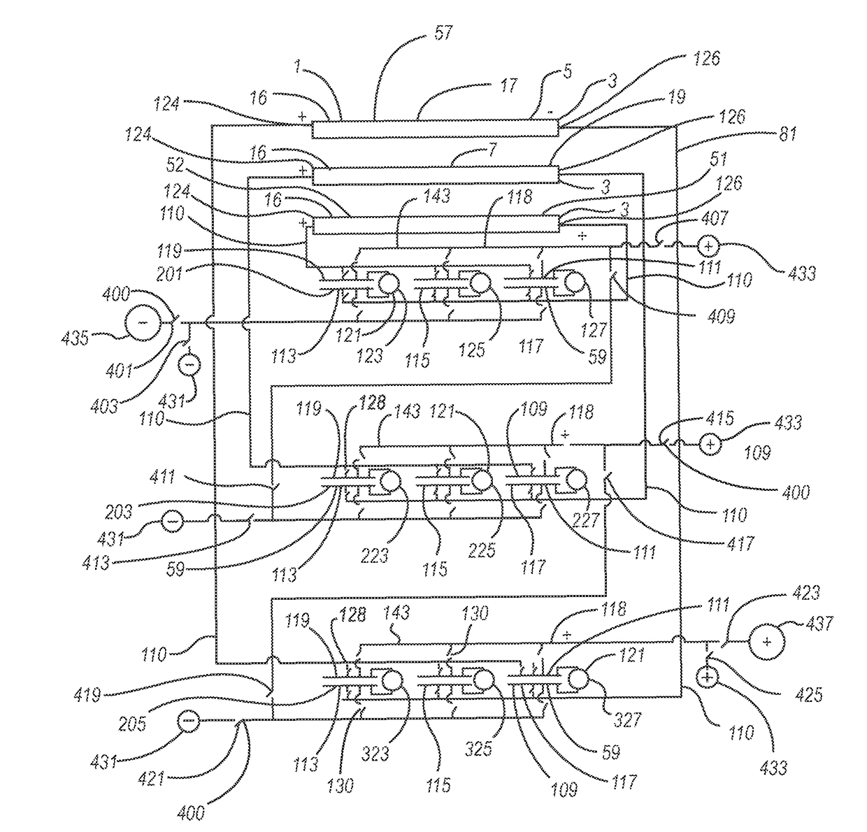
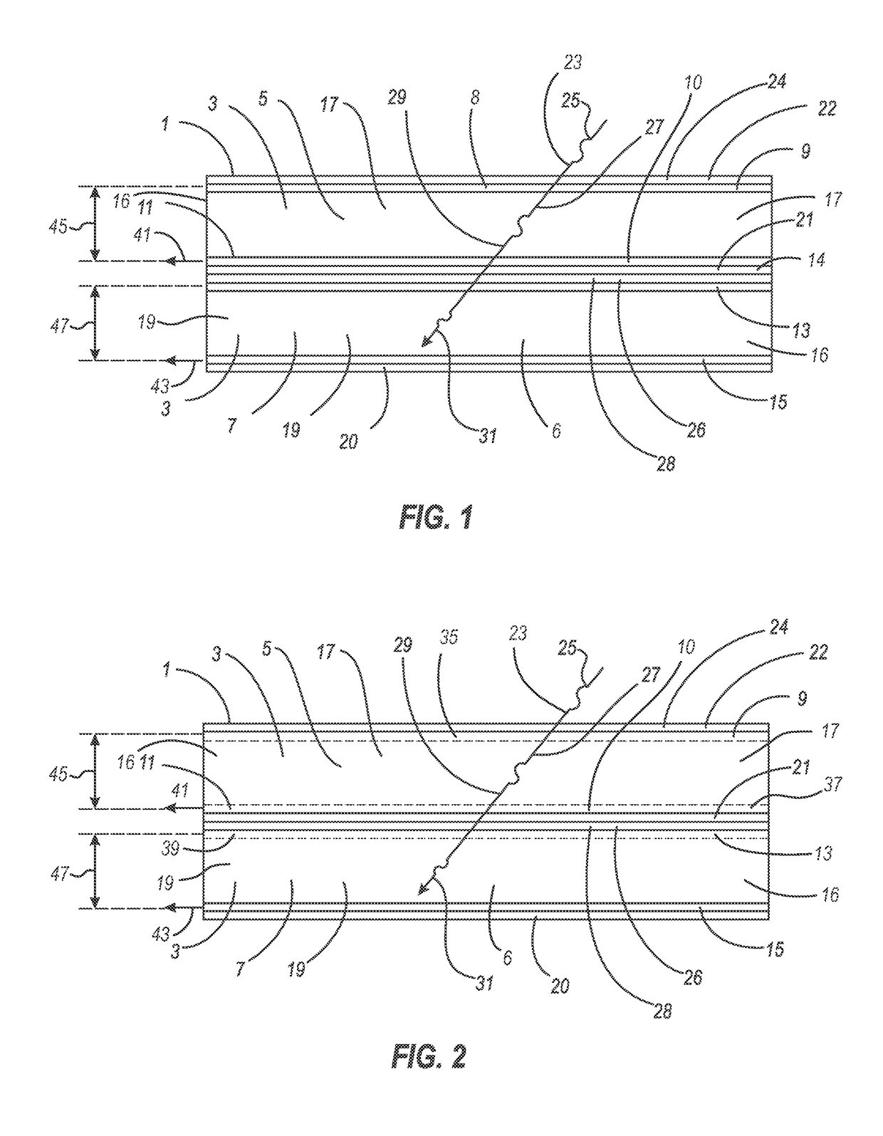
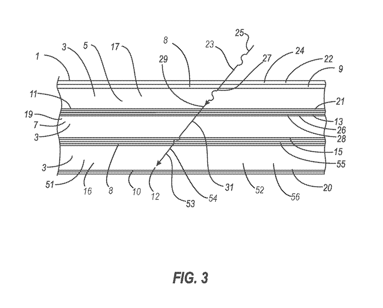
[0047]Referring first to FIG. 1, a schematic cross-section of a preferred embodiment of the multi-element photovoltaic cell 1 of the present invention, having two photovoltaic elements 3, a first photovoltaic element 5 and second photovoltaic element 7, which, for a multi-element photovoltaic cell 1 having two photovoltaic elements 3, is also the last photovoltaic element 6. A first element front conductor 9 and a first element rear conductor 11 are in electrical contact with the first photovoltaic layer 17. Likewise, a second element front conductor 13 and a second element rear conductor 15 are in electrical contact with the second photovoltaic layer 19. The first element front conductor 9, the first photovoltaic layer 17, and the first element rear conductor 11 comprise a photovoltaic element 3, namely the first photovoltaic element 5. The second element front conductor 13, the second photovoltaic layer 19, and the second element rear conductor 15 also comprise a photovoltaic elem...


PUM


Abstract

A multi-element photovoltaic cell having two or more photovoltaic elements with an isolation layer interposed between all contiguous photovoltaic elements. Each photovoltaic element has an element front conductor and an element rear conductor which are in electrical contact with the photovoltaic layer of the photovoltaic element. The current from a respective photovoltaic element which is generated as incident solar radiation irradiates the photovoltaic cell, flows independently of the other photovoltaic elements to one or more capacitor banks controlled by a photovoltaic controller. The photovoltaic controller controls charging and discharging of element capacitors of the capacitor banks so as to optimize the efficiency of the photovoltaic cell.

Description

BACKGROUND OF THE INVENTION[0001]This invention is in the field of photovoltaic cells and in particular in the field of multi-junction, multi-element photovoltaic cells.[0002]Photons of incident solar radiation strike the photovoltaic cells of a solar panel and are absorbed by semiconducting materials, such as silicon. A common type of photovoltaic cell is a single layer silicon cell made from a semiconductor wafer. The photovoltaic material of a photovoltaic cell is commonly formed by doping a thin layer at the top and bottom of the silicon layer of the cell, producing a pn-junction with a particular bandgap energy, Eg. The silicon layer has metallic contacts on the top and bottom. Photons of the incident solar radiation may be reflected or transmitted into the cell. Each of the transmitted photons gives up its energy to an electron, if the energy of the photon is equal to or greater than the bandgap energy, resulting in electrons being excited from their atomic or molecular orbits...

Claims


Application Information

Patent Timeline
Patent Type & Authority Patents(United States)
IPC IPC(8): H02J3/38H02S40/38H02J7/35H01L31/043
CPCH02J3/383H01L31/043H02S40/38H02J7/35Y02E10/566Y02E10/563Y02E10/56Y02E70/30Y02E10/50
Inventor JOHNSON, NELDON P.
Owner BLACK NIGHT ENTERPRISES
Why Eureka
Try Eureka