Small form factor transmitting device

a transmitting device and small form factor technology, applied in the field of optical transmitting devices, can solve problems such as traditional communication transmission overload, and achieve the effects of improving wavelength stability, small first distance, and optimal optical coupling

Active Publication Date: 2018-02-06
LUXNET CORP +1
View PDF5 Cites 2 Cited by
  • Summary
  • Abstract
  • Description
  • Claims
  • Application Information

AI Technical Summary

Benefits of technology

This patent describes a new structure for an optical transmitter package that can improve wavelength stability and focus laser light into a fiber more efficiently. The package includes a thermistor chip, a monitor photodiode chip, and a laser diode chip all on a single submount attached to a thermoelectric cooler module. An optical coupling lens is also included to fix the distance between the laser diode chip and the lens, regardless of changes in temperature. This simplifies calibration and makes it easier to align the transmitter device. The package is designed for easy detachment and recycling of the lens. Additionally, the package structure is convenient for heat dissipation when multiple transmitter devices are assembled.

Problems solved by technology

The communication transmission or reception using the traditional cable is limited to bandwidth and transmission speed of the traditional cable and mass information transmission required in modern life causes the traditional communication transmission overload.
However, such light transmitter structure can emit optical signal with preset frequency which usually lacks stability and often drifts away from the preset wavelength during environmental temperature changes.

Method used


Image

  • Small form factor transmitting device
  • Small form factor transmitting device
  • Small form factor transmitting device

Examples


Embodiment Construction

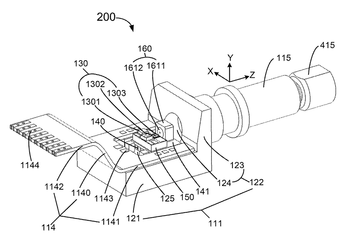
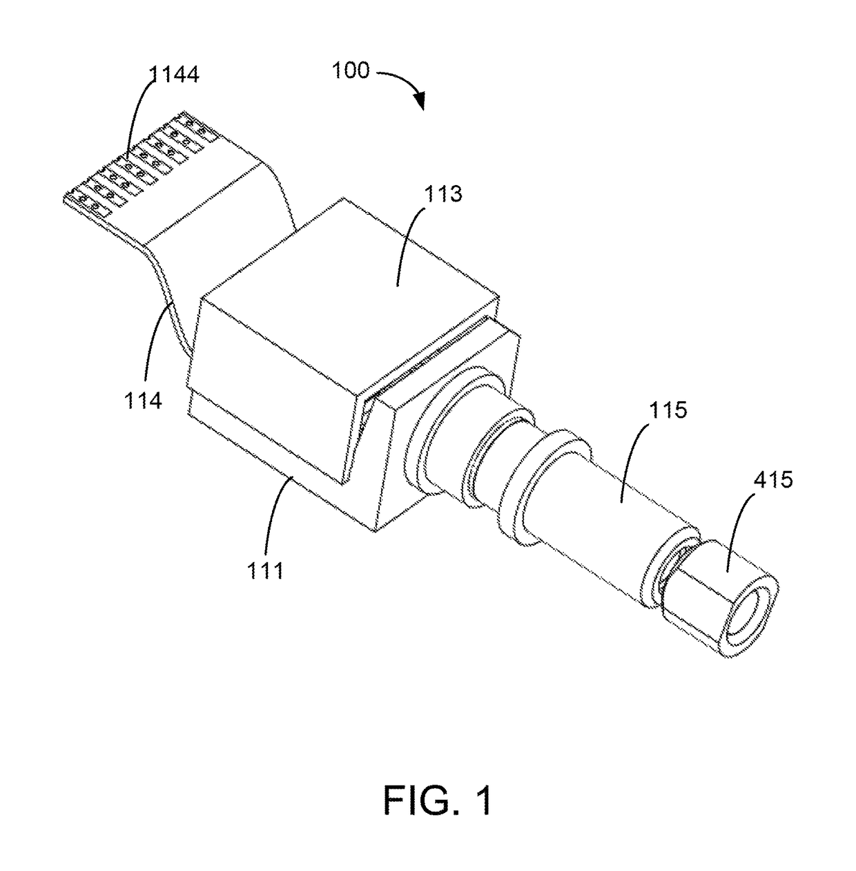
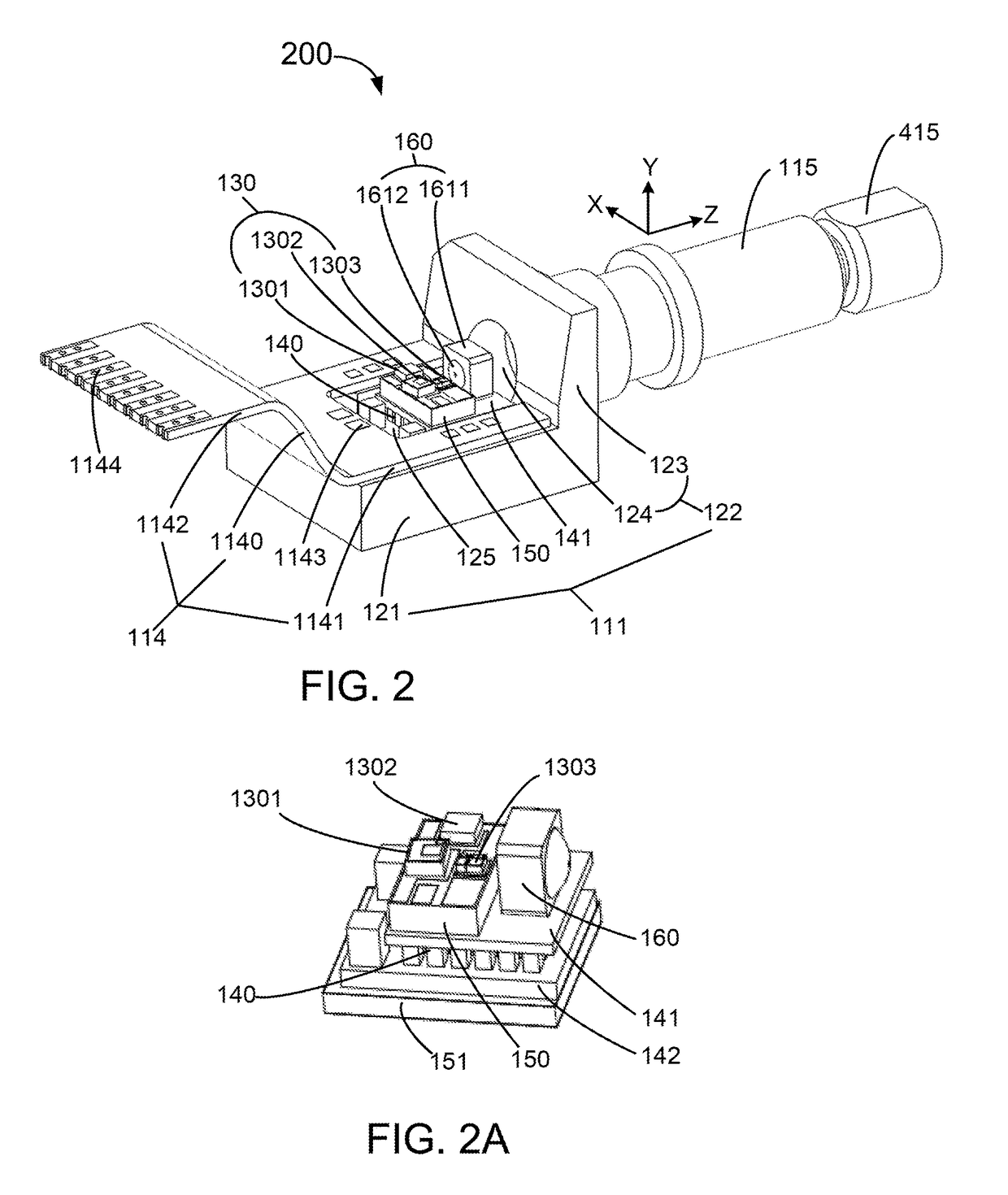
[0021]The present disclosure is related to an optical transmitting device. More particularly, the present invention provides an improved package integrating C-band DFB laser diode chip and a built-in thermoelectric cooler (TEC) module directly on a submount sharing a common cold side of the TEC module with an assembly of an aspherical optical coupling lens. Processes for assembling the optical transmitting device are also disclosed. In certain embodiments, the invention is applied for high bandwidth optical communication, though other applications are possible.

[0022]The following description is presented to enable one of ordinary skill in the art to make and use the invention and to incorporate it in the context of particular applications. Various modifications, as well as a variety of uses in different applications will be readily apparent to those skilled in the art, and the general principles defined herein may be applied to a wide range of embodiments. Thus, the present inventio...


PUM


Abstract

A packaged transmitter device includes a base member comprising a planar part mounted with a thermoelectric cooler, a transmitter, and a coupling lens assembly, and an assembling part connected to one side of the planar part. The device further includes a circuit board bended to have a first end region and a second end region being raised to a higher level. The first end region disposed on a top surface of the planar part includes multiple electrical connection patches respectively connected to the thermoelectric and the transmitter. The second end region includes an electrical port for external connection. Additionally, the device includes a cover member disposed over the planar part. Furthermore, the device includes a cylindrical member installed to the assembling part for enclosing an isolator aligned to the coupling lens assembly along its axis and connected to a fiber to couple optical signal from the transmitter to the fiber.

Description

CROSS-REFERENCE TO RELATED APPLICATIONS[0001]This application is a continuation of and claims priority to U.S. application Ser. No. 14 / 745,316, filed Jun. 19, 2015, commonly assigned and incorporated by reference herein for all purposes.BACKGROUND OF THE INVENTION[0002]The present disclosure is related to an optical transmitting device. More particularly, the present invention provides an improved 1550 nm DFB laser diode package on a submount sharing the cold side of a built-in thermoelectric cooling module with an assembly of an aspherical optical coupling lens. Processes for assembling the optical transmitting device are also disclosed.[0003]As science and technology are updated rapidly, processing speed and capacity of the computer increase correspondingly. The communication transmission or reception using the traditional cable is limited to bandwidth and transmission speed of the traditional cable and mass information transmission required in modern life causes the traditional c...

Claims


Application Information

Patent Timeline
Patent Type & Authority Patents(United States)
IPC IPC(8): H04B10/50G02B6/42H01S5/00H01S5/022H01S5/024H01S5/068H01S5/06H01S5/125
CPCH01S5/0612G02B6/4212G02B6/4271H01S5/0064H01S5/0224H01S5/02284H01S5/02288H01S5/02415H01S5/068H01S5/125H04B10/501G02B6/4204H01S5/02438G02B6/4215G02B6/4287G02B6/4296H01S5/02248H01S5/02325H01S5/02251H01S5/0234H01S5/02253
Inventor NAGARAJAN, RADHAKRISHNAN L.LI, PENG-CHIHLAW, PI-CHENG
Owner LUXNET CORP
Why Eureka
Try Eureka