Manufacture method of TFT substrate and sturcture thereof

a manufacturing method and substrate technology, applied in the field of display technology, can solve the problems of lower response speed, higher driving voltage, higher etc., and achieve the effect of reducing the threshold voltage of flat panel display, reducing the ohm contact resistance, and reducing the power consumption of flat panel display

Active Publication Date: 2018-02-20
TCL CHINA STAR OPTOELECTRONICS TECH CO LTD
View PDF7 Cites 0 Cited by
  • Summary
  • Abstract
  • Description
  • Claims
  • Application Information

AI Technical Summary

Benefits of technology

[0008]An objective of the present invention is to provide a manufacture method of an oxide semiconductor TFT substrate capable of improving the ohm contact between the oxide semiconductor layer and the source / the drain and the ohm contact between the pixel electrode layer and the source / the drain to reduce the ohm contact resistance. The threshold voltage of the flat panel display can be reduced, and accordingly the power consumption of the flat panel display can be effectively reduced and the response speed thereof can be raised.
[0009]Another objective of the present invention is to provide an oxide semiconductor TFT substrate structure, which the ohm contact resistance between the oxide semiconductor layer and the source / the drain and the ohm contact resistance between the pixel electrode layer and the source / the drain are smaller to lower the threshold voltage of the flat panel display and the power consumption of the flat panel display and to make the response speed faster.
[0031]The benefits of the present invention are: according to the manufacture method of the oxide semiconductor TFT structure of the present invention, by locating the second heavily doped transparent conducting thin film layer and the third heavily doped transparent conducting thin film layer at the upper, lower surfaces of the source / the drain, it is capable of promoting the ohm contact between the oxide semiconductor layer and the source / the drain and the ohm contact between the pixel electrode layer and the source / the drain to reduce the ohm contact resistance. The threshold voltage of the flat panel display can be reduced, and accordingly the power consumption of the flat panel display can be effectively reduced and the response speed thereof can be raised; according to the oxide semiconductor TFT structure of the present invention, with the second heavily doped transparent conducting thin film layer and the third heavily doped transparent conducting thin film layer at the upper, lower surfaces of the source / the drain, the ohm contact resistance between the oxide semiconductor layer and the source / the drain and the ohm contact resistance between the pixel electrode layer and the source / the drain can be smaller to lower the threshold voltage of the flat panel display and the power consumption of the flat panel display and to make the response speed faster.

Problems solved by technology

However, the ohm contact resistance between the oxide semiconductor layer and the source / the drain, the ohm contact resistance between the pixel electrode layer and the source / the drain are larger and leads to higher driving voltage, higher power consumption and lower response speed of the flat panel display.

Method used


Image

  • Manufacture method of TFT substrate and sturcture thereof
  • Manufacture method of TFT substrate and sturcture thereof
  • Manufacture method of TFT substrate and sturcture thereof

Examples


Embodiment Construction

[0042]In order to better understand the characteristics and technical aspect of the invention, please refer to the following detailed description of the present invention is concerned with the diagrams.

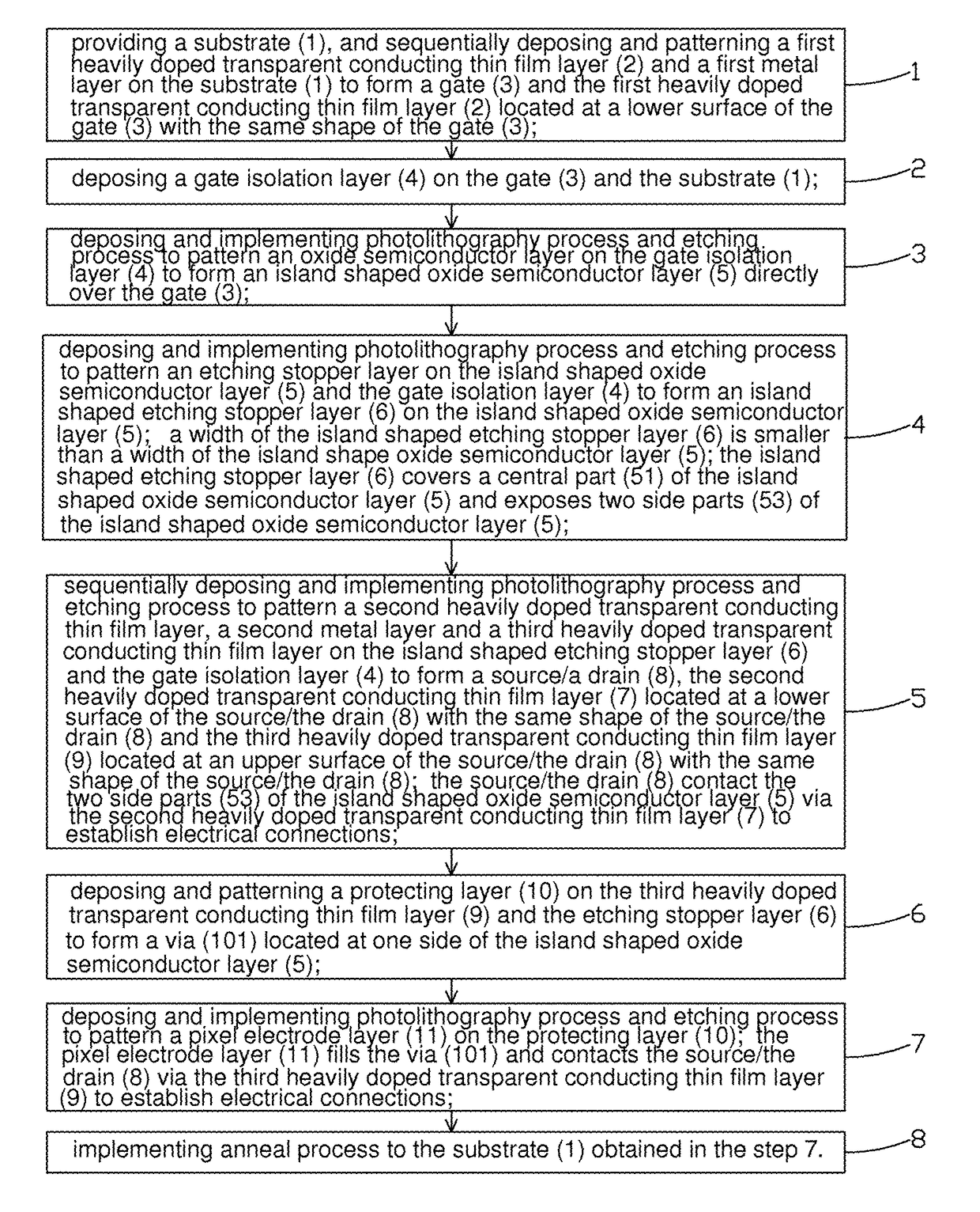
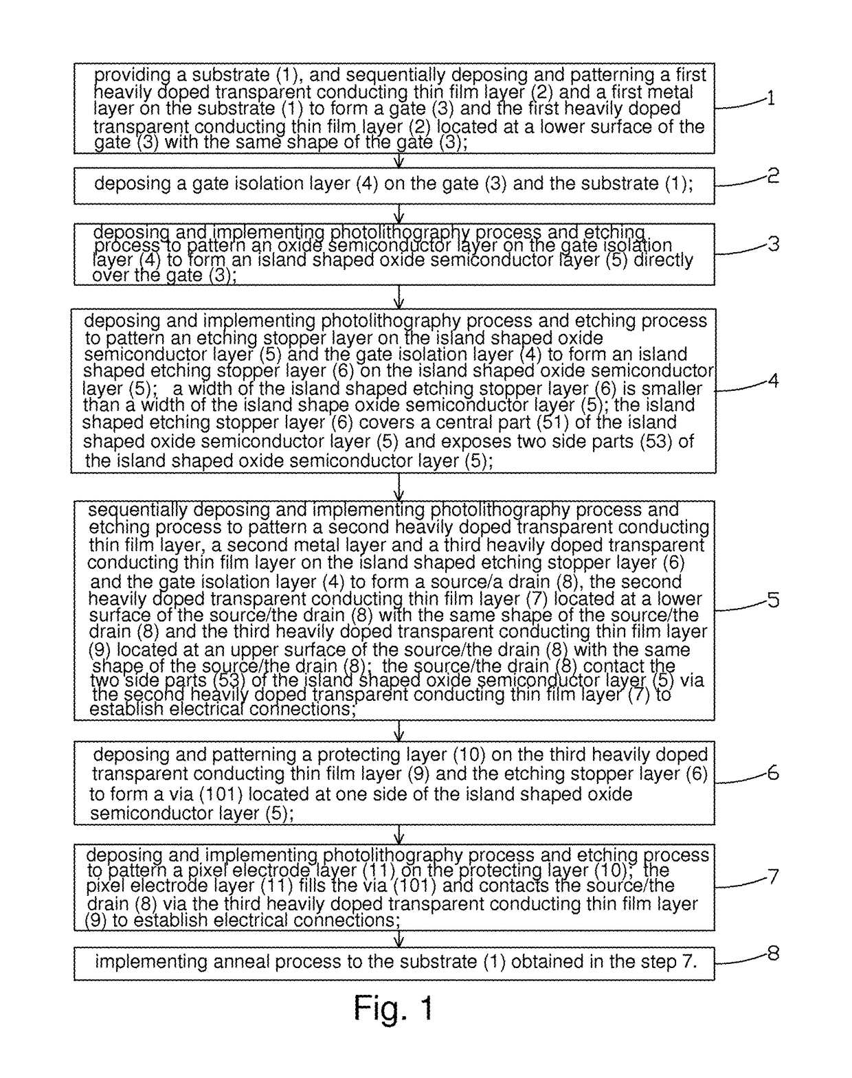
[0043]Please refer to FIG. 1, which is a flowchart of a manufacture method of an oxide semiconductor TFT substrate according to the present invention, comprising steps of:

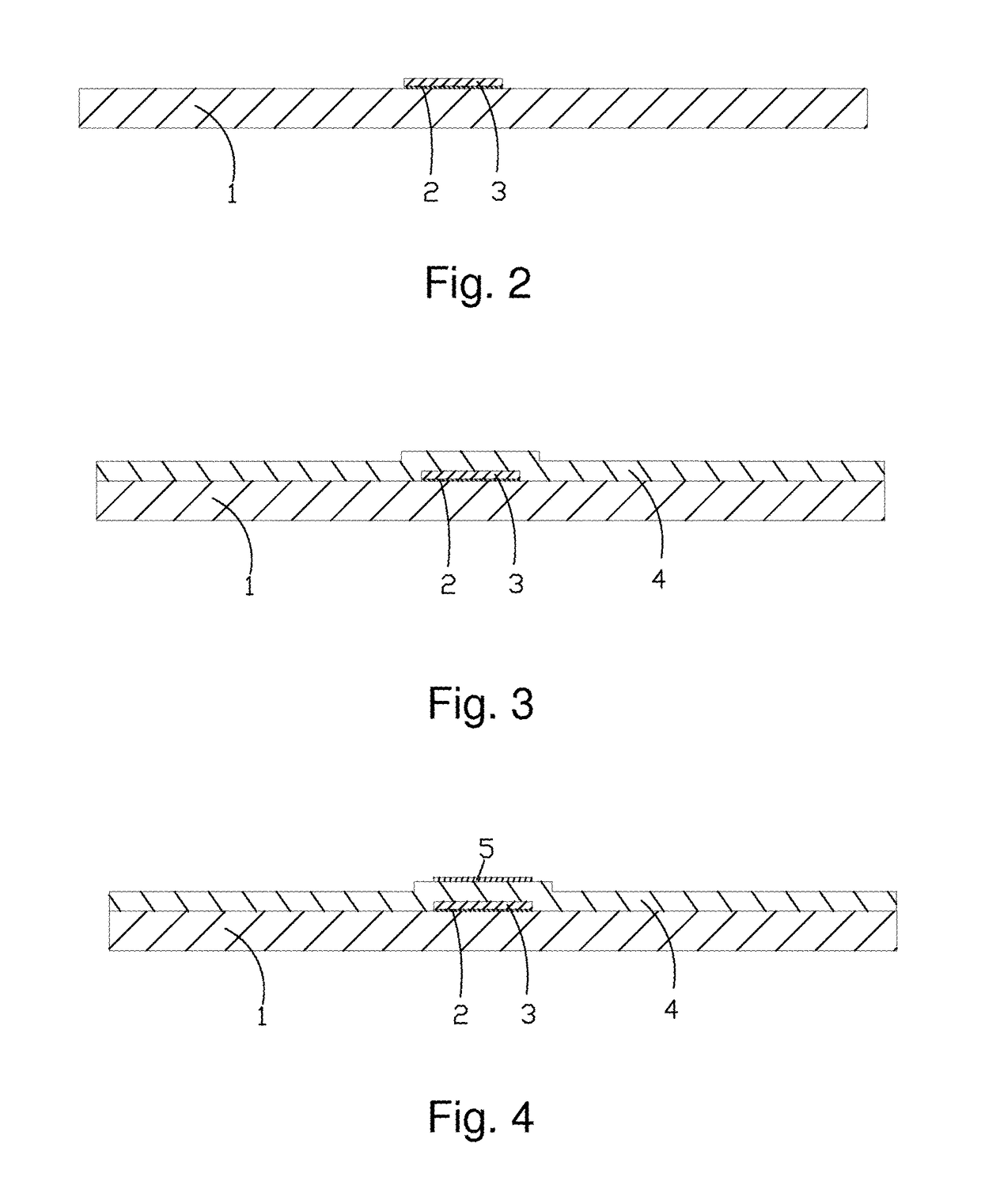
[0044]step 1, please refer to FIG. 2, providing a substrate 1, and sequentially deposing and patterning a first heavily doped transparent conducting thin film layer 2 and a first metal layer on the substrate 1 to form a gate 3 and the first heavily doped transparent conducting thin film layer 2 located at a lower surface of the gate 3 with the same shape of the gate 3.

[0045]The substrate 1 is a transparent substrate. Preferably, the substrate 1 is a glass substrate.

[0046]In the step 1, the photolithography process is implemented with one general mask, and then the etching process is implemented to pattern the first h...


PUM

PropertyMeasurementUnit
thicknessaaaaaaaaaa
thicknessaaaaaaaaaa
thicknessaaaaaaaaaa

Abstract

The present invention provides a manufacture method of an oxide semiconductor TFT substrate, and the method comprises steps of: 1, forming a gate (3) and a first heavily doped transparent conducting thin film layer (2) on a substrate (1); 2, deposing a gate isolation layer (4); 3, forming an island shaped oxide semiconductor layer (5); 4, forming an island shaped photoresistor layer (6); 5, forming a source / a drain (8), and a second, a third heavily doped transparent conducting thin film layer (7, 9), and the source / the drain (8) contact the two side parts (53) of the island shaped oxide semiconductor layer (5) via the second heavily doped transparent conducting thin film layer (7) to establish electrical connections; 6, deposing and patterning a protecting layer (10); 7, deposing and patterning a pixel electrode layer (11) which contacts the source / the drain (8) via the third heavily doped transparent conducting thin film layer (9) to establish electrical connections; 8, implementing anneal process.

Description

FIELD OF THE INVENTION[0001]The present invention relates to a display technology field, and more particularly to a manufacture method of an oxide semiconductor TFT substrate and a structure thereof.BACKGROUND OF THE INVENTION[0002]A flat panel display possesses advantages of being ultra thin, power saved and radiation free and has been widely utilized. Present flat panel displays mainly comprise a LCD (Liquid Crystal Display) or an OLED (Organic Light Emitting Display).[0003]To be compared with a well developed TFT-LCD, an OLED based on the Organic Light Emitting Diodes is an active light emitting display, which possesses outstanding properties of self-illumination, high contrast, wide view angle (up to 170°), fast response, high luminous efficiency, low operation voltage (3-10V), ultra-thin (thickness smaller than 2 mm) and etc. The display devices utilizing OLED technology has possibility to have a lighter, thinner, charming appearance, more excellent color display quality, wider...

Claims


Application Information

Patent Timeline
Patent Type & Authority Patents(United States)
IPC IPC(8): H01L27/12H01L29/786H01L29/423H01L29/417H01L29/66H01L29/45H01L29/49
CPCH01L27/1225H01L27/124H01L27/127H01L27/1248H01L29/41733H01L29/78618H01L29/45H01L29/4908H01L29/66742H01L29/66969H01L29/7869H01L29/42384H01L27/1214H01L27/1288
Inventor WANG, JUN
Owner TCL CHINA STAR OPTOELECTRONICS TECH CO LTD
Why Eureka
Try Eureka