Manufacture method of LTPS array substrate

a manufacturing method and array substrate technology, applied in the field of display technology, can solve the problems of complex manufacturing process of the entire ltps array substrate, small volume of ltps semiconductor elements, and high integration, and achieve the effect of great electrical properties

Active Publication Date: 2018-04-03
WUHAN CHINA STAR OPTOELECTRONICS TECH CO LTD
View PDF13 Cites 4 Cited by
  • Summary
  • Abstract
  • Description
  • Claims
  • Application Information

AI Technical Summary

Benefits of technology

[0015]An objective of the present invention is to provide a manufacture method of a LTPS array substrate, which can effectively reduce the manufacture cost of the LTPS array substrate, and the manufactured LTPS array substrate possesses great electrical property.
[0055]The benefits of the present invention are: the present invention provides a manufacture method of a LTPS array substrate. By utilizing one halftone mask, the N type heavy doping, the channel doping of the first polysilicon layer of the NMOS region and the P type heavy doping of the second polysilicon layer of the PMOS region, the three processes which previously require three masks are integrated into one mask process, and two exposure processes are eliminated, which significantly raises the exposure capacity, and meanwhile saves the manufacture cost of two masks to effectively reduce the manufacture cost of the LTPS array substrate, and the manufactured LTPS array substrate possesses great electrical property.

Problems solved by technology

However, on the other hand, the volume of the LTPS semiconductor element is small and the integration is high.
The manufacture process of the entire LTPS array substrate is complicated, and the production cost is higher.
The manufacture process is complicated and the production cost is high.

Method used


Image

  • Manufacture method of LTPS array substrate
  • Manufacture method of LTPS array substrate
  • Manufacture method of LTPS array substrate

Examples


Embodiment Construction

[0075]For better explaining the technical solution and the effect of the present invention, the present invention will be further described in detail with the accompanying drawings and the specific embodiments.

[0076]Please refer to FIGS. 7-16, the present invention provides a manufacture method of a LTPS array substrate, comprising steps of:

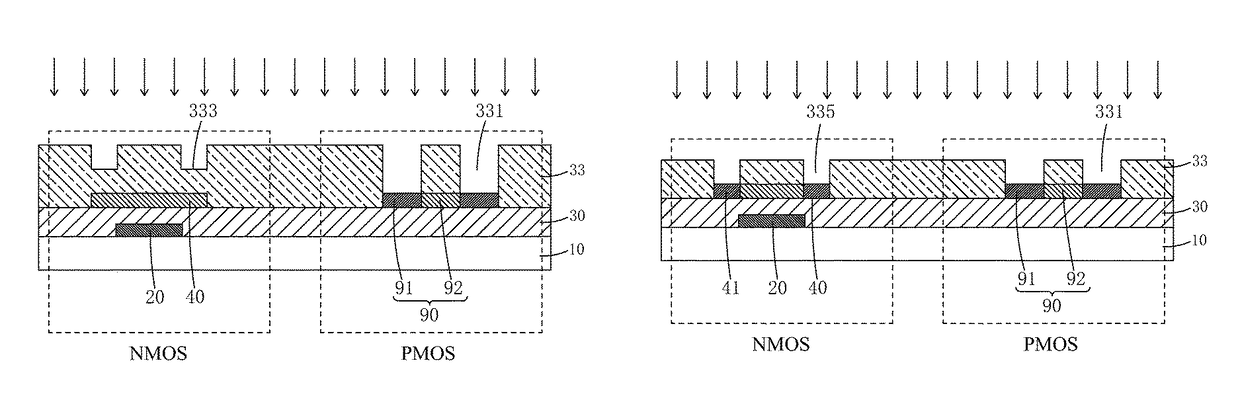
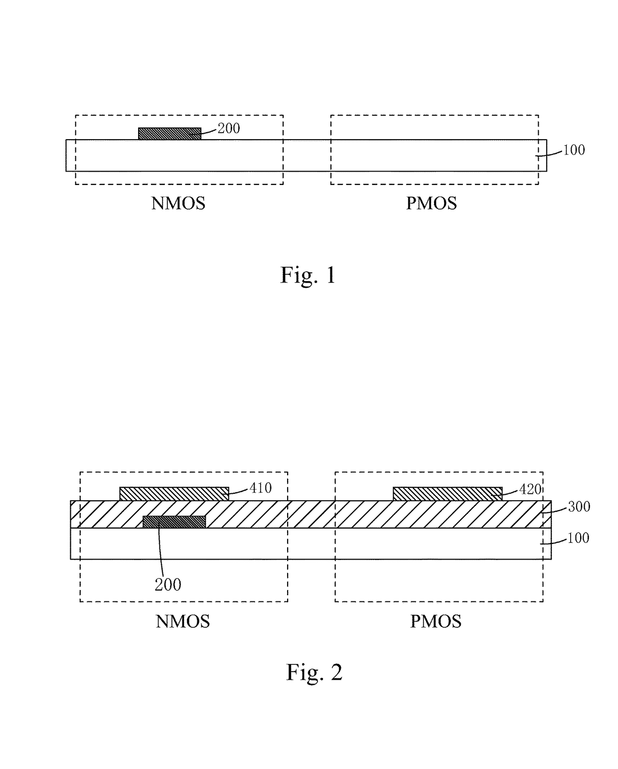
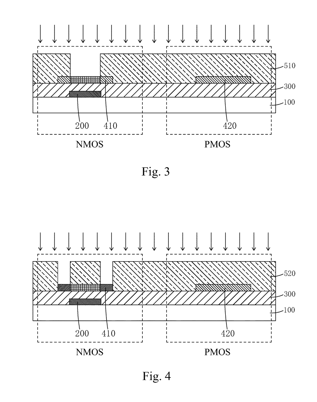
[0077]step 1, as shown in FIG. 7, providing a substrate 10, and defining a NMOS region and a PMOS region on the substrate 10, and depositing a first metal layer on the substrate 10, and patterning the first metal layer to obtain a light shielding layer 20 in the NMOS region.

[0078]step 2, as shown in FIG. 8, forming a buffer layer 30 on the light shielding layer 20 and the substrate 10, and depositing an amorphous silicon layer on the buffer layer 30, and employing a low temperature crystallization process to convert the amorphous silicon layer into the polysilicon layer, and patterning the polysilicon layer to obtain a first polysilicon layer 40 ...


PUM

PropertyMeasurementUnit
thicknessaaaaaaaaaa
transparent conductiveaaaaaaaaaa
temperatureaaaaaaaaaa

Abstract

The present invention provides a manufacture method of a LTPS array substrate. By utilizing one halftone mask, the N type heavy doping, the channel doping of the first polysilicon layer of the NMOS region and the P type heavy doping of the second polysilicon layer of the PMOS region, the three processes which previously require three masks are integrated into one mask process, and two exposure processes are eliminated, which significantly raises the exposure capacity, and meanwhile saves the manufacture cost of two masks to effectively reduce the manufacture cost of the LTPS array substrate, and the manufactured LTPS array substrate possesses great electrical property.

Description

FIELD OF THE INVENTION[0001]The present invention relates to a display technology field, and more particularly to a manufacture method of a LTPS array substrate.BACKGROUND OF THE INVENTION[0002]With the development of display technology, the flat panel device, such as Liquid Crystal Display (LCD) possesses advantages of high image quality, power saving, thin body and wide application scope. Thus, it has been widely applied in various consumer electrical products, such as mobile phone, television, personal digital assistant, digital camera, notebook, laptop, and becomes the major display device.[0003]Most of the liquid crystal displays on the present market are back light type liquid crystal displays, which comprise a liquid crystal display panel and a back light module. Generally, the liquid crystal display panel comprises a CF (Color Filter) substrate, a TFT (Thin Film Transistor) substrate, a LC (Liquid Crystal) sandwiched between the CF substrate and the TFT substrate and sealant...

Claims


Application Information

Patent Timeline
Patent Type & Authority Patents(United States)
IPC IPC(8): H01L27/12G02F1/1335G02F1/1362H01L21/77
CPCH01L27/1288G02F1/133514H01L27/1274H01L27/1222G02F1/136209G02F1/1362H01L21/77G02F1/136231G02F1/136236H01L29/66757H01L29/78621H01L29/78633H01L27/1277H01L27/1285
Inventor HE, CHAO
Owner WUHAN CHINA STAR OPTOELECTRONICS TECH CO LTD
Why Eureka
Try Eureka