Hall sensor and compensation method for offset caused by temperature distribution in hall sensor

a temperature distribution and sensor technology, applied in the field of hall sensors, can solve the problems of increasing chip size, low resistance, and inability to completely cancel the offset voltage, so as to reduce the chip size, reduce the cost, and reduce the distance between the heat source and the hall element.

Inactive Publication Date: 2018-04-17
ABLIC INC
View PDF7 Cites 5 Cited by
  • Summary
  • Abstract
  • Description
  • Claims
  • Application Information

AI Technical Summary

Benefits of technology

[0018]In view of the above, the present invention has an object to provide a Hall sensor including elements serving as heat sources out of components of a circuit for driving a Hall element, and capable of cancelling an offset by spinning current even when a temperature distribution is generated in the Hall element due to the influence of heat generation without an increase in chip area caused by addition of a complex compensation circuit or enlarged separation between elements.
[0027]Moreover, a Hall sensor is provided in which an offset voltage can be eliminated, the chip size can be reduced, and the cost can be suppressed since a complex circuit is not used and the distance between the heat source and the Hall element is not increased.

Problems solved by technology

It is considered that the offset voltage is generated when potential distribution inside the element becomes imbalanced by, for example, mechanical stress applied to the element from the outside or misalignment occurring in a manufacturing process.
However, the offset voltage may not completely be cancelled by this offset cancellation circuit.
However, when this assumption is not satisfied, for example, even when R1=R3 for one direction but this relationship is not established for the other direction, the difference may not be made zero, and hence the offset may not be cancelled.
When the temperature in the Hall element 10 is not uniform, but has a distribution, the resistance in the Hall element 10 is not uniform, either, because the temperature is not uniform, resulting in locations low in the resistance and locations high in the resistance.
Hei 08-330646, but the method uses the plurality of the depletion layer control electrodes and requires a complex control circuit, and hence has such a problem that the chip size increases, which leads to an increase in cost.

Method used


Image

  • Hall sensor and compensation method for offset caused by temperature distribution in hall sensor
  • Hall sensor and compensation method for offset caused by temperature distribution in hall sensor
  • Hall sensor and compensation method for offset caused by temperature distribution in hall sensor

Examples


Embodiment Construction

[0034]A detailed description is now given of an embodiment of the present invention with reference to the drawings.

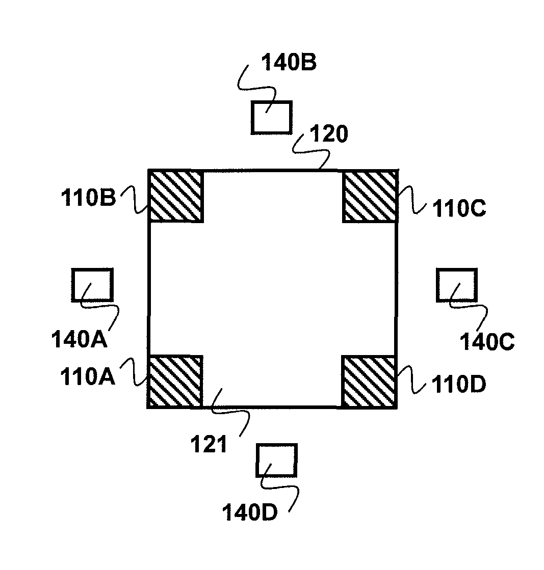
[0035]FIG. 1 is a plan view of a Hall sensor according to the embodiment of the present invention. The Hall sensor includes a Hall element for sensing magnetism and a circuit for driving or controlling the Hall element.

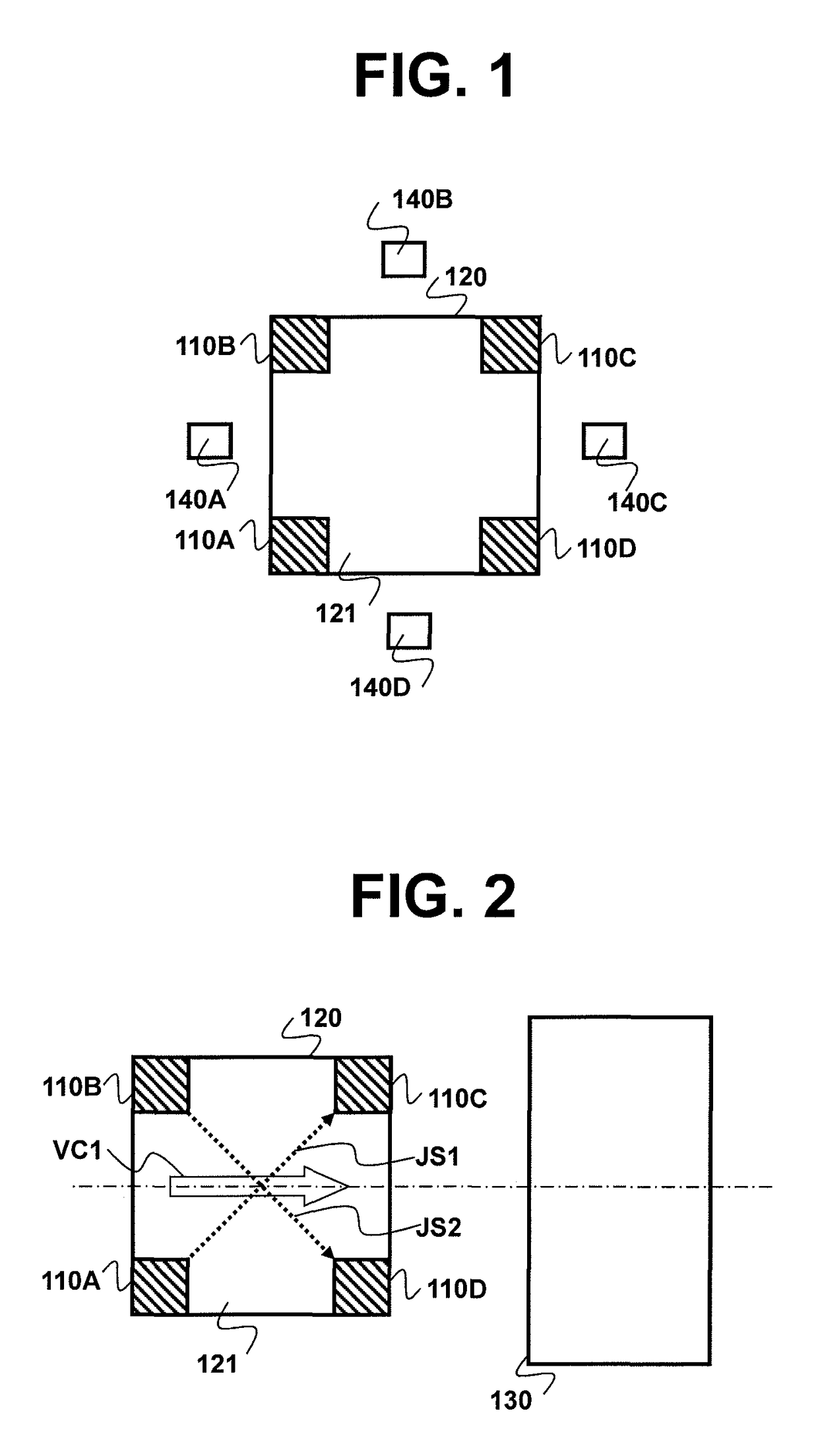
[0036]First, a description is given of a plan shape of the Hall element. As illustrated in FIG. 1, a Hall element 120 includes, on a semiconductor substrate, a magnetism sensing portion constructed by a square N-type doped region 121 and control current input terminals and Hall voltage output terminals 110A, 110B, 110C, and 110D constructed by N-type highly-doped regions having the same shape, which are arranged at respective vertices of the square magnetism sensing portion. The Hall element 120 is shaped into the square, resulting in a symmetrical Hall element having four axes of symmetry.

[0037]Further, temperature sensors 140A, 140B, 140C, and 140D are ...


PUM


Abstract

In a Hall sensor in which a Hall element and elements serving as heat sources out of components of a circuit for driving the Hall element are arranged close to each other on a silicon substrate, two directions of control currents by spinning current for the Hall element are selected in a vector manner based on signals from temperature sensors arranged close to a periphery of the Hall element, thereby enabling the elimination of a magnetic offset caused by heat generation of the heat sources.

Description

BACKGROUND OF THE INVENTION[0001]1. Field of the Invention[0002]The present invention relates to a semiconductor Hall element and a Hall sensor including a driving circuit for the semiconductor Hall element. In particular, the present invention relates to a Hall sensor capable of eliminating an offset voltage.[0003]2. Description of the Related Art[0004]At first the principle of detection of the presence of a magnetic field by a Hall element is described. When a magnetic field is applied perpendicularly to a current flowing through a substance, an electric field (Hall voltage) is generated in a direction perpendicular to both the current and the magnetic field. The principle of the magnetic detection by the Hall element is to acquire an intensity of the magnetic field based on a magnitude of the Hall voltage.[0005]FIG. 3 is a diagram for illustrating the principle of an ideal Hall effect. On an ideal Hall element, a Hall voltage VH as an output from a voltmeter 3 is represented as:V...

Claims


Application Information

Patent Timeline
Patent Type & Authority Patents(United States)
IPC IPC(8): G01R33/00G01R33/07
CPCG01R33/0017G01R33/07G01R33/007G01R33/0005G01R33/0029
Inventor HIOKA, TAKAAKIAKINO, MASARU
Owner ABLIC INC
Why Eureka
Try Eureka