Chemical mechanical planarization apparatus and methods

a mechanical planarization and chemical technology, applied in the direction of manufacturing tools, lapping machines, electric circuit machining, etc., can solve the problems of deteriorating the formation of patterns, such as devices, and structures

Active Publication Date: 2018-04-24
SEMICON MFG INT (BEIJING) CORP +1
View PDF22 Cites 13 Cited by
  • Summary
  • Abstract
  • Description
  • Claims
  • Application Information

AI Technical Summary

Benefits of technology

[0017]As a consumable supply of a CMP process, a polishing slurry may have a significantly important effect on the planarization results of the CMP process. The polishing slurry may normally consist of polish particles and chemical additives, etc. A microscopic view of the CMP process may include a chemical process and a physical process. During the chemical process, a chemical reaction may happen between the chemicals in the polishing slurry and the to-be-polished layer on a wafer; and easy-be-removed products may be produced by the chemical reaction. During the physical process, physical scratches may happen between the polishing particles and the to-be-polished layer; and the products from the chemical process may be removed. The polishing particles in the existing polish slurry may be often silicon dioxide particles. The silicon oxide particles in the polishing slurry may have a negative zeta potential, while the polishing pad and the surface of the wafer may have a positive zeta potential, thus the silicon dioxide particles may be absorbed on the polishing pad and the surface of the wafer. It may be difficult to remove the absorbed silicon dioxide particles by de-ionized (DI) water, thus residual silicon oxide particles may be formed on the wafer and the polishing pad after the CMP process. The residual silicon oxide particles on the wafer may affect the performance of the subsequently formed semiconductor devices. Further, the residual silicon oxide particles on the polishing pad may scratch the subsequent to-be-polished wafers. According to the disclosed apparatus and methods, the silicon oxide particle residue issue and other issues may be overcome by using an alkaline solution in the CMP process and / or a negative power source in the CMP apparatus.
[0021]In one embodiment, as shown in FIG. 2, in order to obtain a better polishing result, a plurality of grooves may be formed in the polishing layer 303. The depth of the grooves may be smaller than the thickness of the polishing pad 303. The width of the grooves may be in a range of approximately 0.5 mm˜1 mm. When a negative voltage is applied on the metal layer 302 of the polishing pad 304, the negative interface potential on the bottom of the grooves may relatively stronger, thus it may generate stronger electrical repulsion on the polishing particles; and the formation of the residual polishing particles may be prevented. In certain other embodiments, other appropriate patterns may be formed in the polishing layer 303 to prevent the residual polishing particles.
[0036]In one embodiment, the basic solution, for example, an alkaline solution may be sprayed onto the surface of the polishing pad 304; and a negative voltage may be applied on the metal layer 302 of the polishing pad 304. The alkaline solution may increase the pH value of the polishing slurry; and increase the repulsion between the polishing particles of the polishing slurry, thus the agglomeration of the polishing particles may be prevented. The alkaline solution may also increase the repulsion of the polishing pad 304 onto the polishing particles, thus the polishing particle may be expelled into a solution; and the formation of the residual polishing particles may be prevented. Further, the metal layer 302 of the polishing pad 304 may connect with the negative power source 315, thus a negative voltage may be uniformly distributed on the surface of the metal layer 302; and a uniform negative potential may be formed on the surface of the polishing layer 303. Such a negative potential may generate an electrical repulsion to the polishing particles with a negative zeta potential, thus the formation of the residual polishing particles on the surface of the polishing pad 304 may be prevented. In one embodiment, providing the alkaline solution and applying a negative voltage may be performed simultaneously, thus the residual and / or the absorbed polishing particles on the surface of the polishing pad 304 may be rapidly and effectively removed; and the performance of the CMP process may be improved.
[0030]Further, referring to FIG. 2, the basic solution supply port 309 may supply a basic solution onto the surface of the polishing pad 304. The basic solution may be used to increase the pH value of the polishing slurry. The increased pH value of the polishing slurry may increase the repulsion between the polishing particles; and prevent the polishing particles from agglomerating. Further, the increased pH value may also increase the electric repulsion of the polishing pad 304 to the polishing particles. Thus, the polishing particles on the surface of the polish pad 304 may be expelled into a solution; and the formation of the residual polishing particles may be prevented.

Problems solved by technology

However, the multiple-layered layout technique may cause the surface of the silicon wafer to be uneven, and it may deteriorate the formation of the patterns, such as devices, and structures, etc.
However, during the CMP process, the CMP apparatus may scratch the to-be-polished wafer; thus it may need further improvements on the performance of the existing CMP apparatus.

Method used


Image

  • Chemical mechanical planarization apparatus and methods
  • Chemical mechanical planarization apparatus and methods
  • Chemical mechanical planarization apparatus and methods

Examples


Embodiment Construction

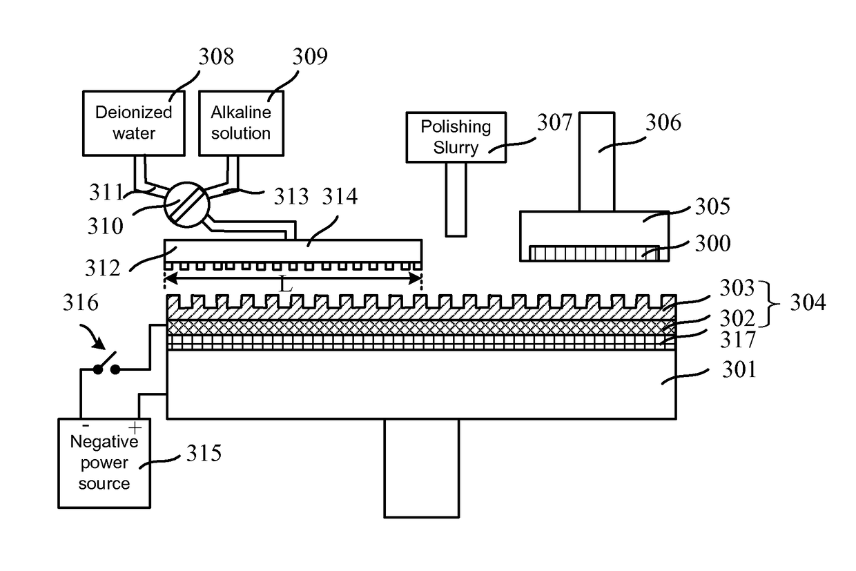
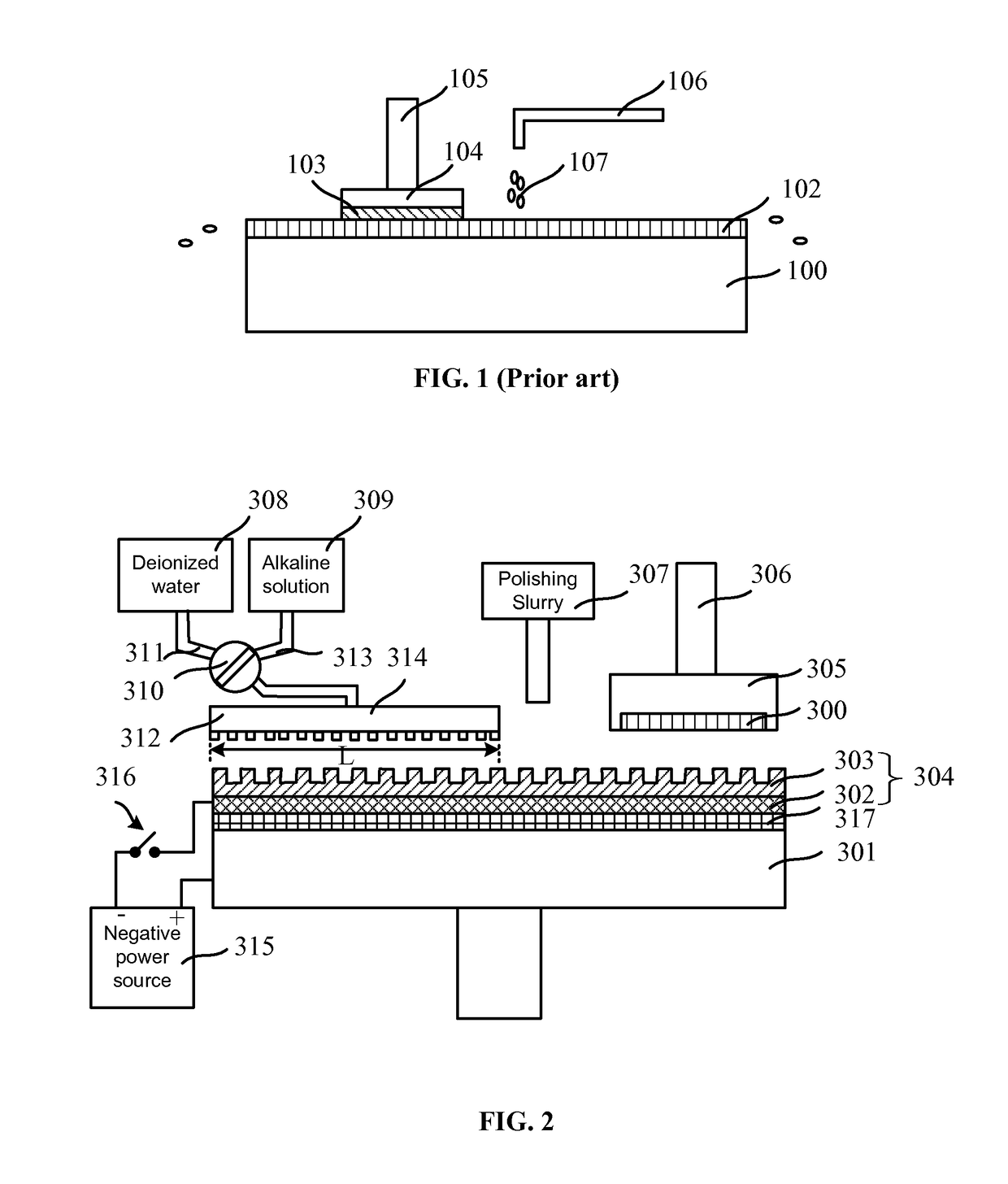
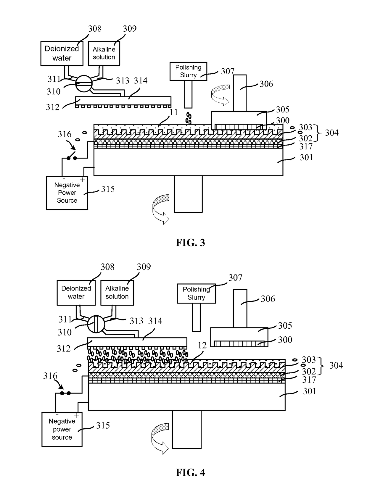
[0016]Reference will now be made in detail to exemplary embodiments of the invention, which are illustrated in the accompanying drawings. Wherever possible, the same reference numbers will be used throughout the drawings to refer to the same or like parts.

[0017]As a consumable supply of a CMP process, a polishing slurry may have a significantly important effect on the planarization results of the CMP process. The polishing slurry may normally consist of polish particles and chemical additives, etc. A microscopic view of the CMP process may include a chemical process and a physical process. During the chemical process, a chemical reaction may happen between the chemicals in the polishing slurry and the to-be-polished layer on a wafer; and easy-be-removed products may be produced by the chemical reaction. During the physical process, physical scratches may happen between the polishing particles and the to-be-polished layer; and the products from the chemical process may be removed. Th...


PUM

PropertyMeasurementUnit
voltageaaaaaaaaaa
widthaaaaaaaaaa
voltageaaaaaaaaaa

Abstract

A chemical mechanical planarization (CMP) apparatus is provided. The CMP apparatus includes at least one platen; and a polishing pad disposed on the platen. The CMP apparatus also includes a polishing head disposed above the platen and configured to clamp a to-be-polished wafer; and a basic solution supply port disposed above the platen and configured to supply a basic solution onto a surface of the polishing pad. Further, the CMP apparatus includes a slurry arm disposed above the platen and configured to supply a polish slurry on the surface of the polishing pad; and a deionized water supply port configured to supply deionized water onto the surface of the polishing pad. Further, the CMP apparatus also includes a negative power source configured to apply a negative voltage onto the surface of the polishing pad.

Description

CROSS-REFERENCES TO RELATED APPLICATIONS[0001]This application claims the priority of Chinese patent application No. 201310744276.6, filed on Dec. 30, 2013, the entirety of which is incorporated herein by reference.FIELD OF THE INVENTION[0002]The present invention generally relates to the field of semiconductor manufacturing technology and, more particularly, relates to chemical mechanical planarization apparatus and chemical mechanical planarization methods thereof.BACKGROUND[0003]With the rapid development of ultra large scale integration (ULSI), the fabrication process of integrate circuits (ICs) has become more and more complex; and more and more precise. In order to increase the integration level and lower the production cost, the number of the devices in a unit area has been increasing. Thus, it has been difficult to lay out lines (interconnect structure, etc) in one plane, i.e., two-dimensional layout; and a multiple-layered layout technique has been adapted to utilize the ve...

Claims


Application Information

Patent Timeline
Patent Type & Authority Patents(United States)
IPC IPC(8): B24B37/04H01L21/306B24B57/02H01L21/321H01L21/67B24B37/20B24B37/24B23H3/02B24D3/00H05K3/07B23H7/14
CPCB24B37/04B24B37/044B24B37/046B24B57/02H01L21/30625B23H3/02B23H7/14B24B37/20B24B37/24B24D3/00H01L21/3212H01L21/32115H01L21/32125H01L21/6715H01L21/67051H05K3/07
Inventor DENG, WUFENG
Owner SEMICON MFG INT (BEIJING) CORP
Why Eureka
Try Eureka