Solder joint material and method of manufacturing the same, soldering member and solar cell module
a technology of solder joint and soldering member, which is applied in the direction of manufacturing tools, soldering apparatus, superimposed coating process, etc., can solve the problems of increasing the melting point of solder, reducing the bondability, and reducing the bondability, so as to achieve excellent solder bondability and joint reliability.
- Summary
- Abstract
- Description
- Claims
- Application Information
AI Technical Summary
Benefits of technology
Problems solved by technology
Method used
Image
Examples
example 1
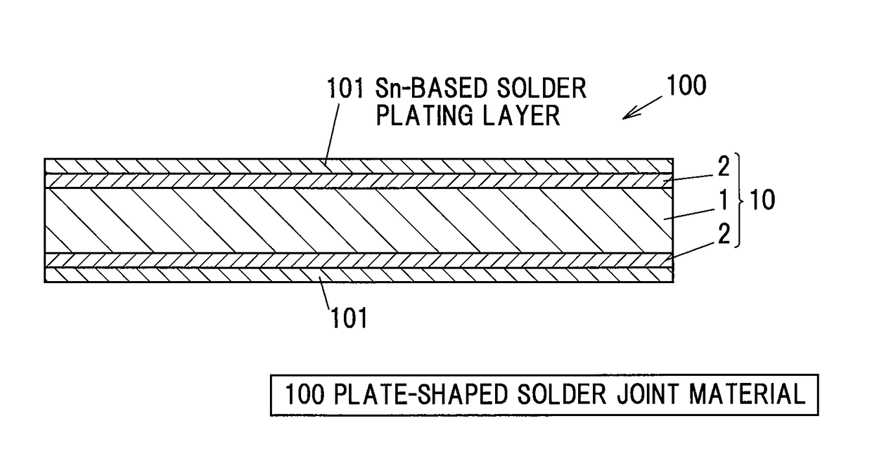
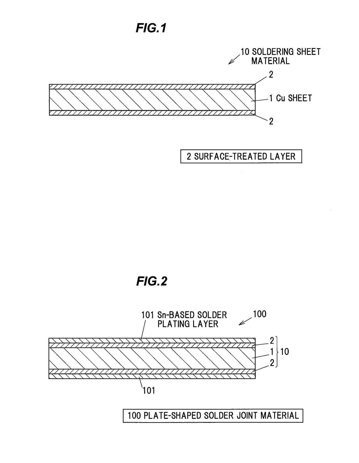
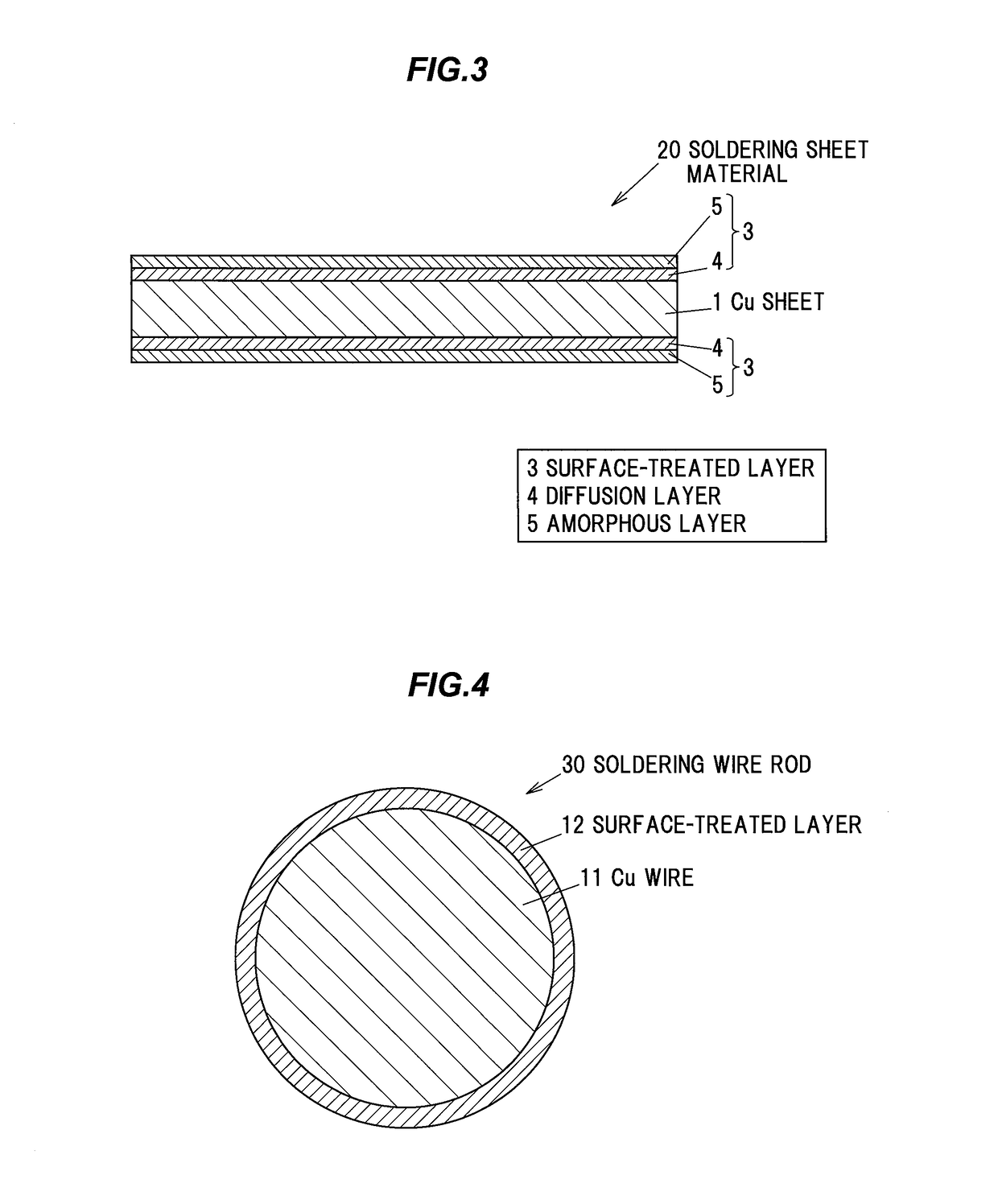
[0107]In Example 1, a 0.5 mm-thick flat sheet of TPC was prepared, a 0.008 μm-thick Zn layer was then formed on a surface of the flat sheet by electrolytic plating and heat treatment was subsequently performed in the ambient air at a temperature of 100° C. for 5 minutes, thereby obtaining a sample. Based on Auger analysis performed on the obtained sample from the surface in a depth direction, it was confirmed that a 0.01 μm-thick surface-treated layer composed of zinc (Zn), oxygen (O) and copper (Cu) was formed.
example 2
[0108]In Example 2, a 0.5 mm-thick flat sheet formed of TPC was prepared, a 0.04 μm-thick Zn layer was then formed on a surface of the flat sheet by electrolytic plating and heat treatment was subsequently performed in the ambient air at a temperature of 120° C. for 10 minutes, thereby obtaining a sample. Based on Auger analysis performed on the obtained sample from the surface in a depth direction, it was confirmed that a 0.05 μm-thick surface-treated layer composed of zinc (Zn), oxygen (O) and copper (Cu) was formed.
example 3
[0109]In Example 3, a 0.5 mm-thick flat sheet formed of TPC was prepared, a 0.08 μm-thick Zn layer was then formed on a surface of the flat sheet by electrolytic plating and heat treatment was subsequently performed in the ambient air at a temperature of 300° C. for 5 seconds, thereby obtaining a sample. Based on Auger analysis performed on the obtained sample from the surface in a depth direction, it was confirmed that a 0.1 μm-thick surface-treated layer composed of zinc (Zn), oxygen (O) and copper (Cu) was formed.
PUM
| Property | Measurement | Unit |
|---|---|---|
| thickness | aaaaa | aaaaa |
| thickness | aaaaa | aaaaa |
| temperature | aaaaa | aaaaa |
Abstract
Description
Claims
Application Information


