Solder joint material and method of manufacturing the same, soldering member and solar cell module

a technology of solder joint and soldering member, which is applied in the direction of manufacturing tools, soldering apparatus, superimposed coating process, etc., can solve the problems of increasing the melting point of solder, reducing the bondability, and reducing the bondability, so as to achieve excellent solder bondability and joint reliability.

Inactive Publication Date: 2015-06-04
HITACHI METALS LTD
View PDF12 Cites 6 Cited by
  • Summary
  • Abstract
  • Description
  • Claims
  • Application Information

AI Technical Summary

Benefits of technology

[0035]According to one embodiment of the invention, a solder joint material can be provided that is excellent in solder bondability and joint reliability after soldering, as well as a method of manufacturing the older joint material, a soldering member, and a solar cell module using the solder joint material or the soldering member.

Problems solved by technology

The method disclosed in WO2009 / 051255 may cause an increase in a melting point of the solder.
Therefore, a problem may arise that the bondability decreases when processed at a lower temperature so as to, e.g., reduce a load applied to components on a substrate during reflow.
However, due to the poor molten metal flow, the bondability may decrease even in this case.

Method used


Image

  • Solder joint material and method of manufacturing the same, soldering member and solar cell module
  • Solder joint material and method of manufacturing the same, soldering member and solar cell module
  • Solder joint material and method of manufacturing the same, soldering member and solar cell module

Examples


first embodiment

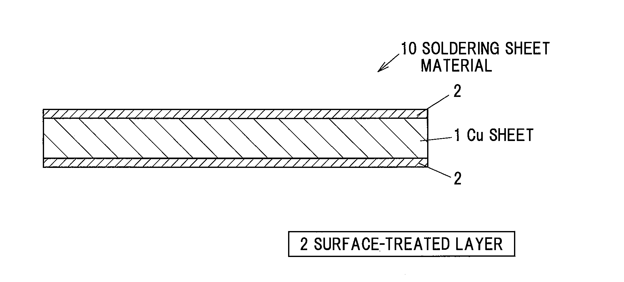
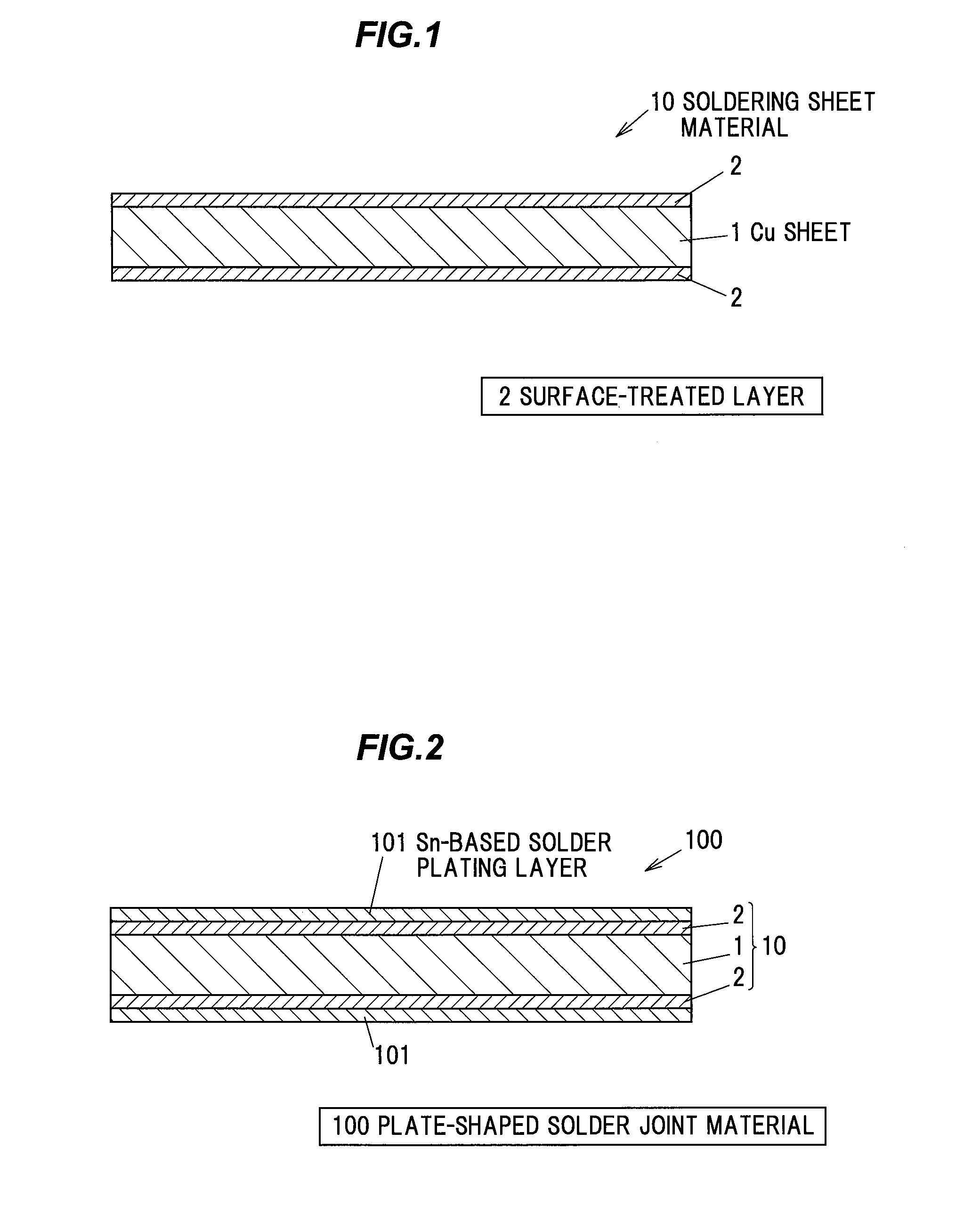
[0048]A solder joint material in the first embodiment of the invention has a plate-like shape in which the surface-treated layer and the Sn-based solder plating layer are sequentially provided on each of a pair of opposing sides of the Cu-based metal sheet which has a rectangular cross section. The layers here are provided on both sides of the Cu-based metal sheet but it is not limited thereto. The surface-treated layer and the Sn-based solder plating layer may be sequentially provided on only one side of the Cu-based metal sheet.

[0049]FIG. 1 is a schematic cross sectional view showing a soldering member in the first embodiment of the invention and FIG. 2 is a schematic cross sectional view showing a solder joint material in the first embodiment of the invention. FIG. 3 is a schematic cross sectional view showing a modification of the soldering member in the first embodiment of the invention.

[0050]A soldering sheet material (soldering member) 10 shown in FIG. 1 is provided with a Cu...

second embodiment

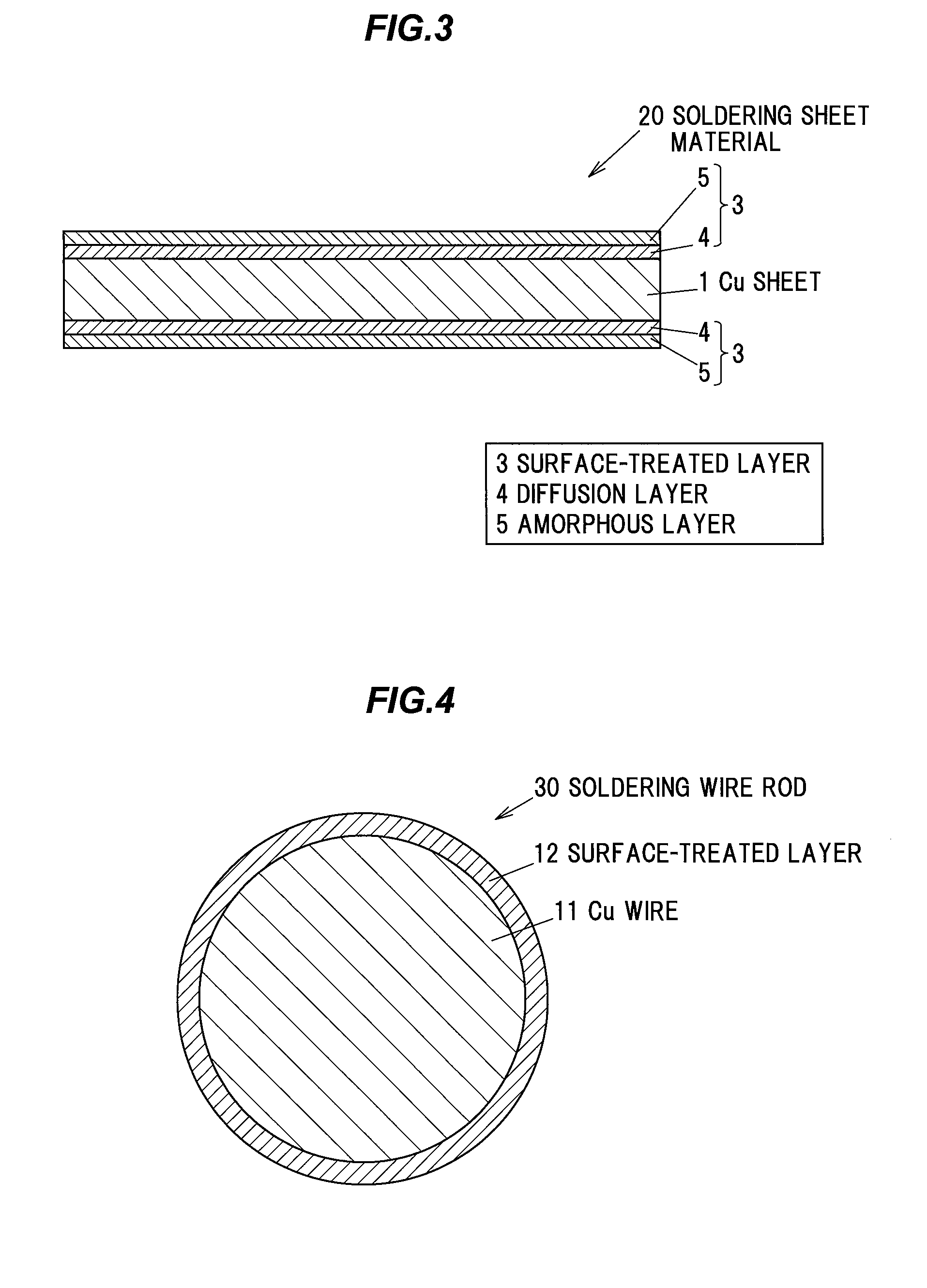
[0070]A solder joint material in the second embodiment of the invention has a wire-like shape in which the surface-treated layer covers an outer periphery of the Cu-based metal material having a circular cross section and the Sn-based solder plating layer covers an outer periphery of the surface-treated layer.

[0071]FIG. 4 is a schematic cross sectional view showing a soldering member in the second embodiment of the invention and FIG. 5 is a schematic cross sectional view showing a solder joint material in the second embodiment of the invention. FIG. 6 is a schematic cross sectional view showing a modification of the soldering member in the second embodiment of the invention.

[0072]A soldering wire rod (soldering member) 30 shown in FIG. 4 is provided with a columnar Cu-based metal wire 11 (hereinafter, sometimes simply referred as “Cu wire”) having a circular cross section and a surface-treated layer 12 covering the outer periphery of the Cu wire 11. A wire-shaped solder joint materi...

example 1

[0098]In Example 1, a 0.5 mm-thick flat sheet of TPC was prepared, a 0.008 μm-thick Zn layer was then formed on a surface of the flat sheet by electrolytic plating and heat treatment was subsequently performed in the ambient air at a temperature of 100° C. for 5 minutes, thereby obtaining a sample. Based on Auger analysis performed on the obtained sample from the surface in a depth direction, it was confirmed that a 0.01 μm-thick surface-treated layer composed of zinc (Zn), oxygen (O) and copper (Cu) was formed.


PUM

PropertyMeasurementUnit
thicknessaaaaaaaaaa
thicknessaaaaaaaaaa
temperatureaaaaaaaaaa

Abstract

A solder joint material includes a copper-based metal material including mainly a copper, a surface-treated layer that is provided on the copper-based metal material and includes an amorphous layer including oxygen and a metal with a higher oxygen affinity than a copper, and a Sn-based solder plating layer provided on the surface-treated layer.

Description

[0001]The present application is based on Japanese patent application No. 2013-248020 filed on Nov. 29, 2013, the entire contents of which are incorporated herein by reference.BACKGROUND OF THE INVENTION[0002]1. Field of the Invention[0003]The invention relates to a solder joint material and a method of manufacturing the solder joint material, a soldering member and a solar cell module.[0004]2. Description of the Related Art[0005]If a bare copper is used as a soldering member, an oxide film formed hinders wetting of the solder and this results in poor solder bondability.[0006]In addition, a brittle intermetallic compound (Cu6Sn5) layer is formed at an interface between copper and Sn-based solder due to heat during soldering. Cu6Sn5 is a hexagonal crystal at high temperature but transforms into an orthorhombic crystal at low temperature. This causes cracks, etc., to develop and decreases joint reliability after soldering. This applies not only to bare copper but also to Sn-plated cop...

Claims


Application Information

Patent Timeline
Patent Type & Authority Applications(United States)
IPC IPC(8): H01L31/0224B23K35/26B23K35/30C23C30/00C22C9/00C22C13/00C23C28/02B23K35/02B23K35/36
CPCH01L31/022425B23K35/0238B23K35/262B23K35/302C23C30/00C22C9/00C22C13/00C23C28/021B23K35/3602B23K35/0222B23K35/0227B23K35/26B23K35/30B23K35/36C23C10/28Y02B10/10Y02E10/50Y10T428/1266
Inventor SAGAWA, HIDEYUKIFUJITO, KEISUKETSUJI, TAKAYUKIKURODA, HIROMITSU
Owner HITACHI METALS LTD
Why Eureka
Try Eureka