

Photo mask and exposure system
a technology of exposure system and photo mask, which is applied in the field of semiconductor technology, can solve the problems of deteriorating uniformity, defective exposure process, and degrading the quality of a semiconductor device, and achieves the effects of improving image performance, facilitating improvement of aperture, and increasing fineness
- Summary
- Abstract
- Description
- Claims
- Application Information
AI Technical Summary
Benefits of technology
Problems solved by technology
Method used
Image

Examples
first embodiment
[0037]This embodiment provides a photo mask, and a resulting pattern formed through an exposure using the photo mask can have improved fineness, thereby improving accuracy of a formed rectilinear pattern.
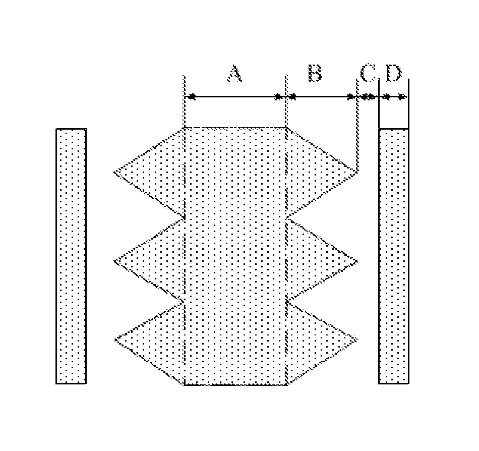
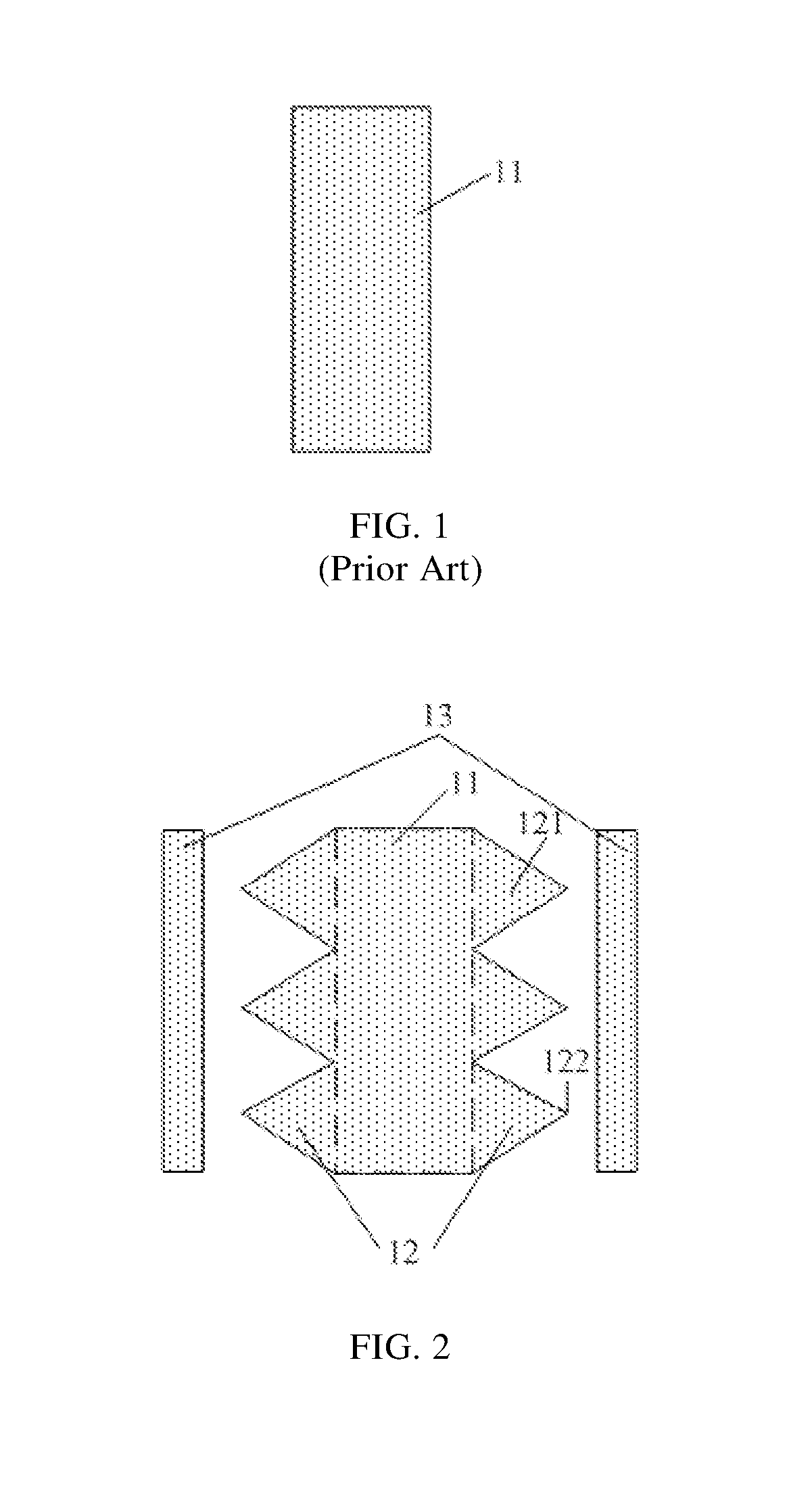
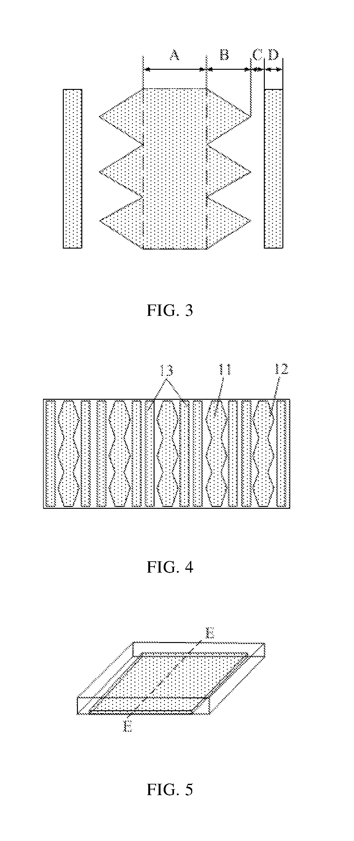
[0038]As shown in FIG. 2, the photo mask is provided with a patterning structure for forming a resulting pattern, the patterning structure includes a strip-like main body 11 for forming a rectilinear pattern and a patterning structure auxiliary unit provided at two sides of the strip-like main body 11, the patterning structure auxiliary unit is able to adjust and compensate direction and intensity of light during exposure, wherein the strip-like main body 11 is used for forming an actual rectilinear pattern, and its length and width are related to the used exposure machine but generally well-matched with those of the actual rectilinear pattern.
[0039]Specifically, the patterning structure auxiliary unit includes a serrated wing part 12 connected to the strip-like main body 11 and a c...
second embodiment
[0054]This embodiment provides a photo mask, which differs from the first embodiment in that only a serrated wing part 12 is provided at the two sides of the strip-like main body 11 in the photo mask of the present embodiment.
[0055]As shown in FIG. 7, the patterning structure auxiliary unit includes the serrated wing part 12 connected with the strip-like main body 11.
[0056]In this embodiment, the shape and structural parameters of the serrated wing part in the photo mask may refer to those in the first embodiment, and are not repeated herein.
[0057]In the photo mask of the present embodiment, by forming the serrated wing part at two sides of the strip-like main body for forming a rectilinear pattern, the resolution of an exposure machine on a micro-pattern is improved, and with the design of the photo mask, the imaging performance is improved without modifying an existing device, and the high PPI property of the exposure machine is fully used, which facilitates improving aperture rat...
third embodiment
[0058]This embodiment provides a photo mask, which differs from the first embodiment in that only a columnar part 13 is provided at the two sides of the strip-like main body 11 in the photo mask of the present embodiment.
[0059]As shown in FIG. 8, the columnar part 13 is provided at an outer side of the strip-like main body 11, is spaced apart from the strip-like main body 11, and includes a first column and a second column symmetric with respect to the strip-like main body 11, bottoms and tops of the first and second columns are substantially level with those of the strip-like main body 11, respectively, and a ratio of the width of the strip-like main body 11 to the width of the first column and / or the second column is in the range of 1:1 to 9:1.
[0060]In this embodiment, the shape and structural parameters of the columnar part in the photo mask may refer to those in the first embodiment, and are not repeated herein.
[0061]In the photo mask of the present embodiment, by forming the co...
PUM
| Property | Measurement | Unit |
|---|---|---|
| apex angle | aaaaa | aaaaa |
| apex angle | aaaaa | aaaaa |
| size | aaaaa | aaaaa |
Abstract
Description
Claims
Application Information