Sealed stacked arrangement of semiconductor devices
What is Al technical title?
Al technical title is built by PatSnap Al team. It summarizes the technical point description of the patent document.
a semiconductor device and stacking technology, applied in semiconductor devices, semiconductor/solid-state device details, instruments, etc., can solve the problems of deteriorating product yield, complicated manufacturing process, and inability to constitute a package using the same size of sub-chips formed in the same manufacturing process, and achieves effective chip mounting, large memory capacity, and the effect of avoiding the loss of heat radiation characteristic of the package and product yield
Inactive Publication Date: 2002-02-05
ELPIDA MEMORY INC
View PDF44 Cites 12 Cited by
Summary
Abstract
Description
Claims
Application Information
AI Technical Summary
This helps you quickly interpret patents by identifying the three key elements:
Problems solved by technology
Method used
Benefits of technology
According to the above means it is possible to provide an effective chip mounting method capable of mounting plural sub chips of the same size without sacrificing the heat radiation characteristic of the package and the product yield. Besides, it is possible to attain large memory capacity and low power consumption of the DRAM package and simplify the manufacturing process for the package. Moreover, it is possible to realize a DRAM package having a memory capacity plural times that of a package comprising a single DRAM chip and thereby expand the limit of memory capacity of DRAM chips; at the same time it is possible to enhance the packaging efficiency of a memory system having a DRAM package as a basic configuration and reduce the cost thereof. Further, it is possible to utilize partial DRAM chips without waste and enhance a substantial product yield of DRAM chips, etc.
Problems solved by technology
However, with progress of higher integration density and larger capacity of semiconductor chips, the present inventors found out that the following problems were involved in the foregoing chip mounting methods.
Therefore, it is impossible to constitute a package using the same size of sub chips formed in the same manufacturing process, like a DRAM chip for example.
In all of these methods, moreover, the manufacturing process is complicated and the product yield is deteriorated in comparison with, for example, the conventional packaging method involving direct wire bonding to a lead frame.
Method used
Image
Click on the blue label to locate the original text in one second.
Reading with bidirectional positioning of images and text.
Examples
Embodiment Construction
1. 128M DRAM Package according to Double Chip Packaging Method
1.1. Outline of DRAM Package
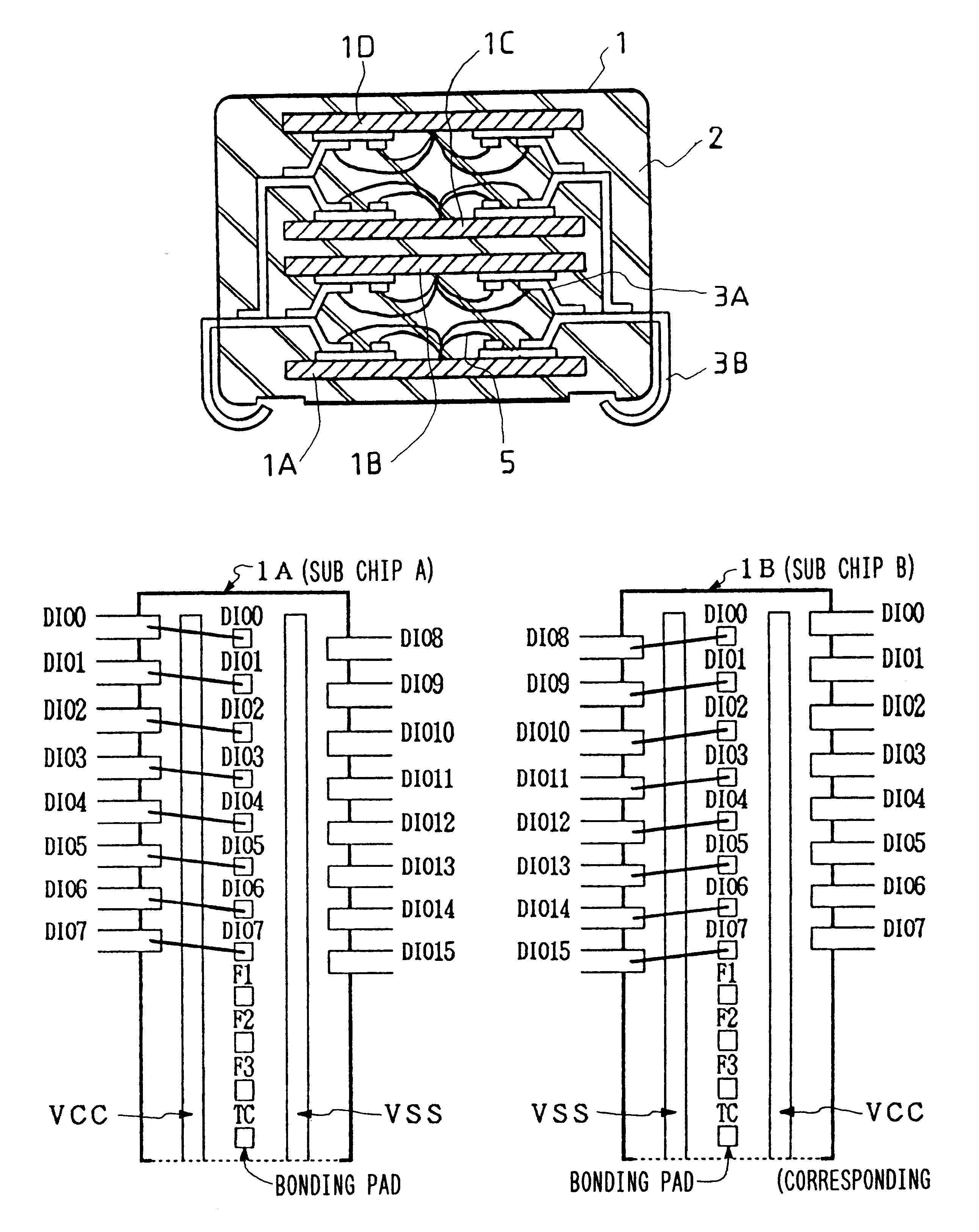
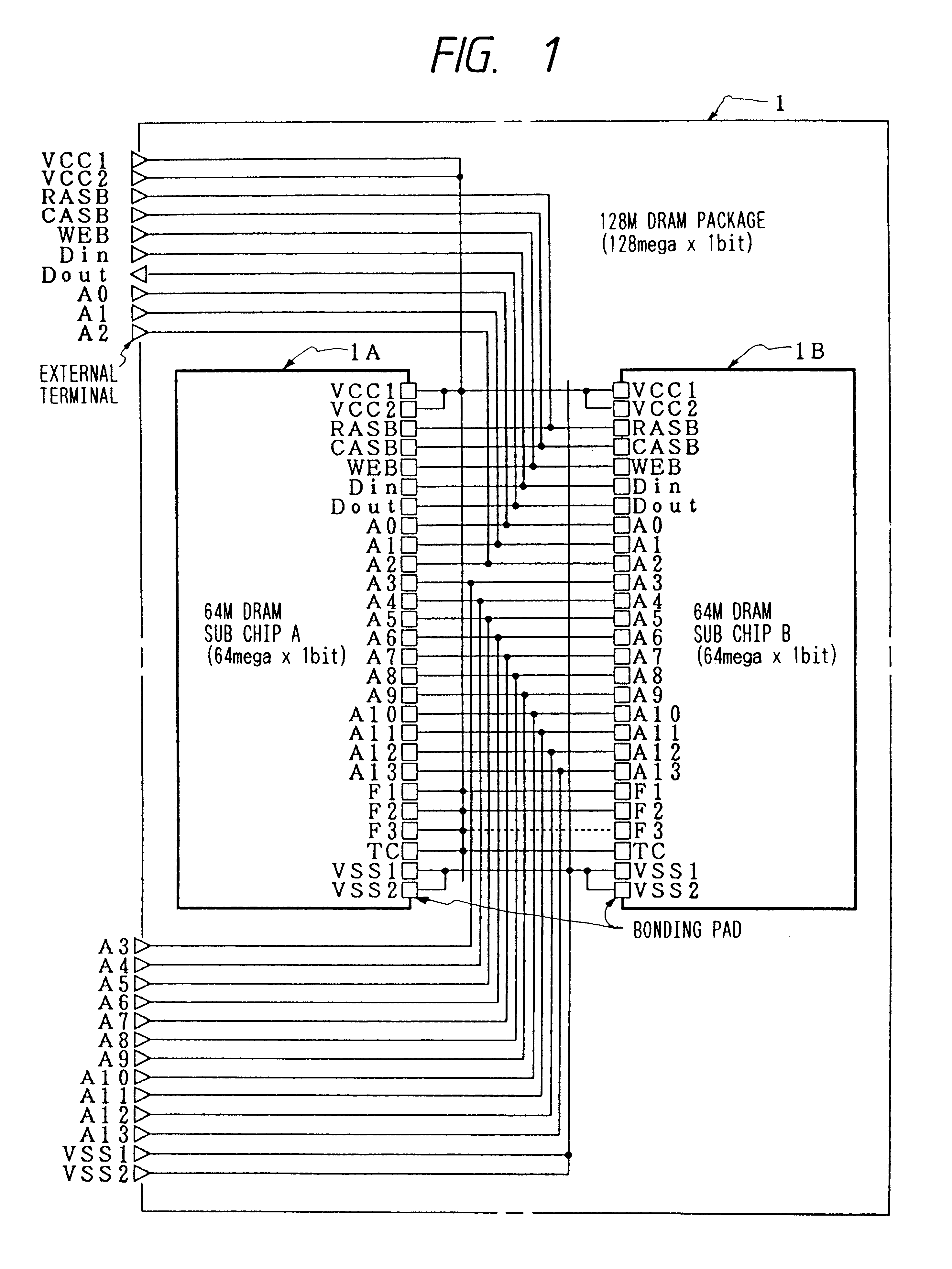
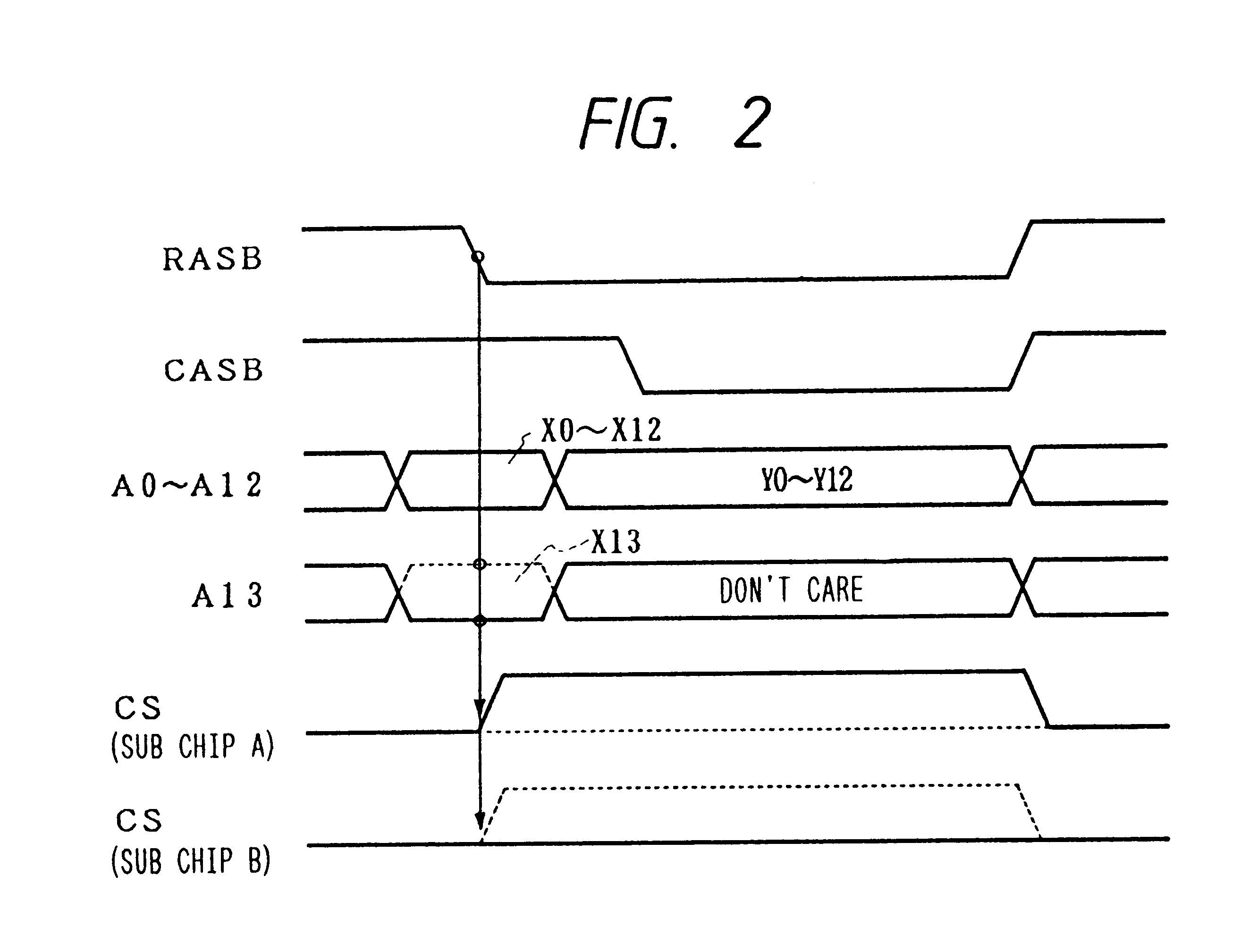
FIG. 1 is a block diagram showing an example of a 128M ("M" or "mega" is assumed equal to the twentieth power of 2 herein) DRAM package according to the present invention, and FIG. 2 is a timing chart in the said DRAM package. With reference to these figures, an outline of this DRAM package and an explanation of a chip selecting method will first be given below. The chip mounting method according to the present invention will herein be designated a double chip packaging method. For a specific description of the double chip packaging method and features thereof, see "1.4. Package Form of DRAM Package."
1.1.1. Block Configuration
A DRAM package 1 according to this embodiment includes two DRAM sub chips 1A and 1B. These sub chips each have a memory capacity of 64 mega. Write data and read data are inputted or outputted each in the unit of one bit through a data input terminal Din or a data output te...
PUM
Abstract
A pair of DRAM chips 1A and 1B are mounted opposedly to each other with wiring means such as lead frames put therebetween, the lead frames being substantially integral with external terminals 3B. Then, these DRAM chips and lead frames are connected together by the conventional wire bonding method. Plural pairs of the thus-connected DRAM chips and lead frames are stacked and corresponding leads of the lead frames are connected in common to form a laminate. The plural DRAM chips thus mounted are activated selectively in accordance with a predetermined chip selection signal. Additionally, partial DRAM chips capable of partially functioning normally are combined together by utilizing the above chip mounting method to constitute a single DRAM package.
Description
BACKGROUND OF THE INVENTIONThe present invention relates to a semiconductor device and a method for manufacturing the same. For example, the present invention is concerned with a DRAM package (a semiconductor device with one or plural DRAM chips mounted thereon will hereinafter be referred to herein as "DRAM package") comprising plural DRAM (Dynamic Random Access Memory) chips (a semiconductor chip capable of functioning as DRAM will hereinafter be referred to herein as "DRAM chip"), as well as a technique which is particularly useful in producing such DRAM package.A DRAM chip having as a basic configuration a memory array comprising lattice-like arranged dynamic memory cells as well as a DRAM package having such DRAM chip as a basic configuration are known. In the conventional DRAM package, usually, one DRAM chip is mounted thereon and bonding pads used therein are connected to corresponding leads of a lead frame integral with external terminals.As to the DRAM package carrying a si...
Claims
Application Information
Patent Timeline
Application Date:The date an application was filed.
Publication Date:The date a patent or application was officially published.
First Publication Date:The earliest publication date of a patent with the same application number.
Issue Date:Publication date of the patent grant document.
PCT Entry Date:The Entry date of PCT National Phase.
Estimated Expiry Date:The statutory expiry date of a patent right according to the Patent Law, and it is the longest term of protection that the patent right can achieve without the termination of the patent right due to other reasons(Term extension factor has been taken into account ).
Invalid Date:Actual expiry date is based on effective date or publication date of legal transaction data of invalid patent.