Supercharge Your Innovation With Domain-Expert AI Agents!

Semiconductor memory device and read and write methods thereof

a memory device and semiconductor technology, applied in the field of semiconductor memory devices, can solve the problems of memory bottlenecks, increase the number of pads in a circuit, and hamper the performance of the computer,

Inactive Publication Date: 2002-06-18
SAMSUNG ELECTRONICS CO LTD
View PDF6 Cites 10 Cited by
  • Summary
  • Abstract
  • Description
  • Claims
  • Application Information

AI Technical Summary

Benefits of technology

Another object of the invention is to improve I / O speed of a semiconductor memory device without increasing the system clock frequency.

Problems solved by technology

This results in a memory bottleneck that hampers performance of the computer.
However, such a method gives rise to the following problems: First, an increment of the chip size follows from the increase in the number of pads in a circuit.
Second, an increment in power consumption follows as well due to the increase of the circuit size, the increased number of the conductors, and the increase in the number of output terminals, each of which should includes a driver having a large load, and so on.
Accordingly, it is not desirable to use the above method to improve the I / O bottleneck in a semiconductor memory.
Consequently, although data having N times the size of the memory port word size can accessed in the memory during one clock period, it is impossible to exchange the data at a speed greater than the frequency of the global clock.
In addition, increasing the frequency of the global clock to improve the bandwidth of the data exchange also increases the operating frequency of the overall memory circuit, thereby incrementing the operating power of the memory.
Further, there is a problem in that the maximum operating frequency of the global clock is limited by the phase difference of the clock generated between each clock wiring of the memory and controller at a specific time.
However, in case of using the memory of FIG. 1, now that all of signals operate in synchronism with the system clock CLK, even if data having N times the memory internal word size can be accessed during a period of one system clock, it is impossible to exchange the data at a speed greater than the frequency of the system clock CLK.
Further, there is a problem in that the maximum operating frequency of the system clock CLK can be limited by the phase difference across the various clock wirings of the memory and controller at a specific time.
Accordingly, simply increasing the system clock frequency is not a promising solution to improving I / O bandwidth.

Method used


Image

  • Semiconductor memory device and read and write methods thereof
  • Semiconductor memory device and read and write methods thereof
  • Semiconductor memory device and read and write methods thereof

Examples


Embodiment Construction

Hereinafter, a preferred embodiment of the present invention will be described in detail with reference to the accompanying drawings. Throughout the drawings, it is noted that the same reference numerals will be used to designate like or equivalent elements having the same function. Further, in the following description, numerous specific details are set forth to provide a more through understanding of the present invention. It will be apparent, however, to one skilled in the art that the present invention may be practiced without these specific details.

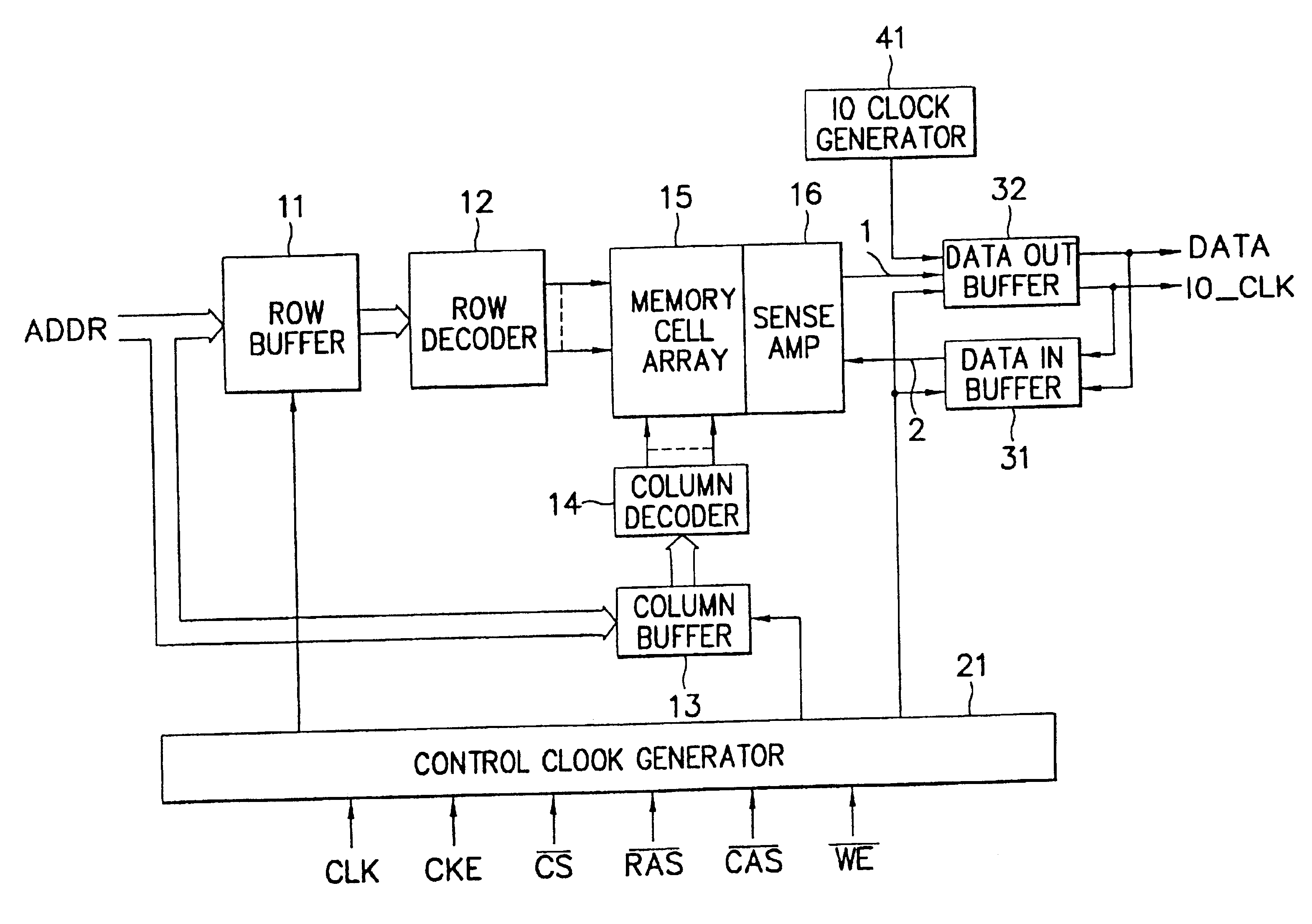
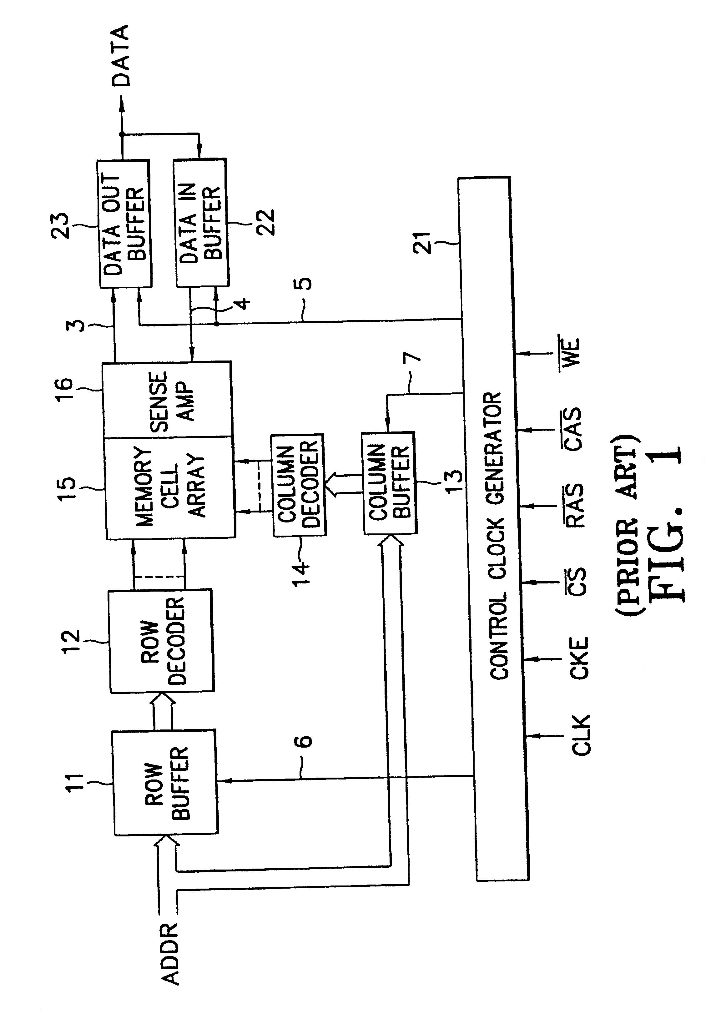
FIG. 3 is a block diagram illustrating the construction of a semiconductor memory device according to the present invention. The detailed description of those elements of FIG. 3 which perform the same functions as the corresponding elements of FIG. 1 will not be repeated.

The most significant difference between the memory of FIG. 1 and the memory of FIG. 3 lies on the construction of a data-in buffer 31 and a data-out buffer 32. First...


PUM


Abstract

A semiconductor memory device includes input / output circuitry capable of operating in sync with an externally provided I / O clock signal. A data in buffer and a data out buffer provide for serial to parallel conversion of write data and, conversely, parallel to serial conversion of read data. The data buffers can be synchronized with the external I / O clock signal thereby decoupling their operation from the internal system clock signal. This strategy improves I / O bandwidth and further provides for matching different numbers of bit lines or word sizes as between the I / O data port and the memory array itself. An internal I / O clock generator can be provided for generating I / O clock signals, again without the limitation of synchronizing to the internal system clock signal.

Description

BACKGROUND OF THE INVENTION1. Field of the InventionThe present-invention relates to a semiconductor memory device and, in particular, to a semiconductor memory device having improved bandwidth input and output using an external synchronous signal and read / write methods thereof.The present application for a semiconductor memory device for exchanging data by using a synchronous signal and read / write methods thereof, is based on Korean Application No. 29574 / 1995 which is incorporated herein by reference for all purposes.2. Description of the Related ArtRecently, while the operating frequency of microprocessors continues to increase in computer systems, the operating frequency of a semiconductor memory device has increased relatively slowly. This results in a memory bottleneck that hampers performance of the computer. One solution for relieving the memory bottleneck is to increase the width of the memory bus so that the amount of the data or word size between the computer and semicondu...

Claims


Application Information

Patent Timeline
Patent Type & Authority Patents(United States)
IPC IPC(8): G11C7/00G11C7/22G11C7/10
CPCG11C7/1006G11C7/1051G11C7/1072G11C7/1078G11C7/1087G11C7/1093G11C7/22
Inventor KYUNG, KYE-HYUN
Owner SAMSUNG ELECTRONICS CO LTD
Features
  • R&D
  • Intellectual Property
  • Life Sciences
  • Materials
  • Tech Scout
  • Unparalleled Data Quality
  • Higher Quality Content
  • 60% Fewer Hallucinations
Learn More