Method for fabricating semiconductor thin film

a technology of silicon semiconductor and thin film, which is applied in the direction of semiconductor devices, coatings, transistors, etc., can solve the problems of low heat resistance, low cost, and high cost of quartz substrate, and achieve the effect of suppressing metal element deviation and facilitating the removal of silicon film

Inactive Publication Date: 2003-10-07
SEMICON ENERGY LAB CO LTD
View PDF24 Cites 29 Cited by
  • Summary
  • Abstract
  • Description
  • Claims
  • Application Information

AI Technical Summary

Benefits of technology

To facilitate the removal of the silicon film for the absorption of the metal element, it is effective to form an oxide film on the crystalline silicon film. Since the oxide film has a selectivity with respect to an etchant (for example, hydradine and ClF.sub.3), the oxide film can serve as an etching stopper.
Further, on a surface of the crystalline silicon film (first silicon film) crystallized with the action of the m...

Problems solved by technology

However, a method for crystallizing am amorphous silicon film by heat treatment in the prior art has the following problem.
However, the quartz substrate is expensive and cannot be used in the liquid crystal electro-opti...

Method used


Image

  • Method for fabricating semiconductor thin film
  • Method for fabricating semiconductor thin film
  • Method for fabricating semiconductor thin film

Examples


embodiment 1

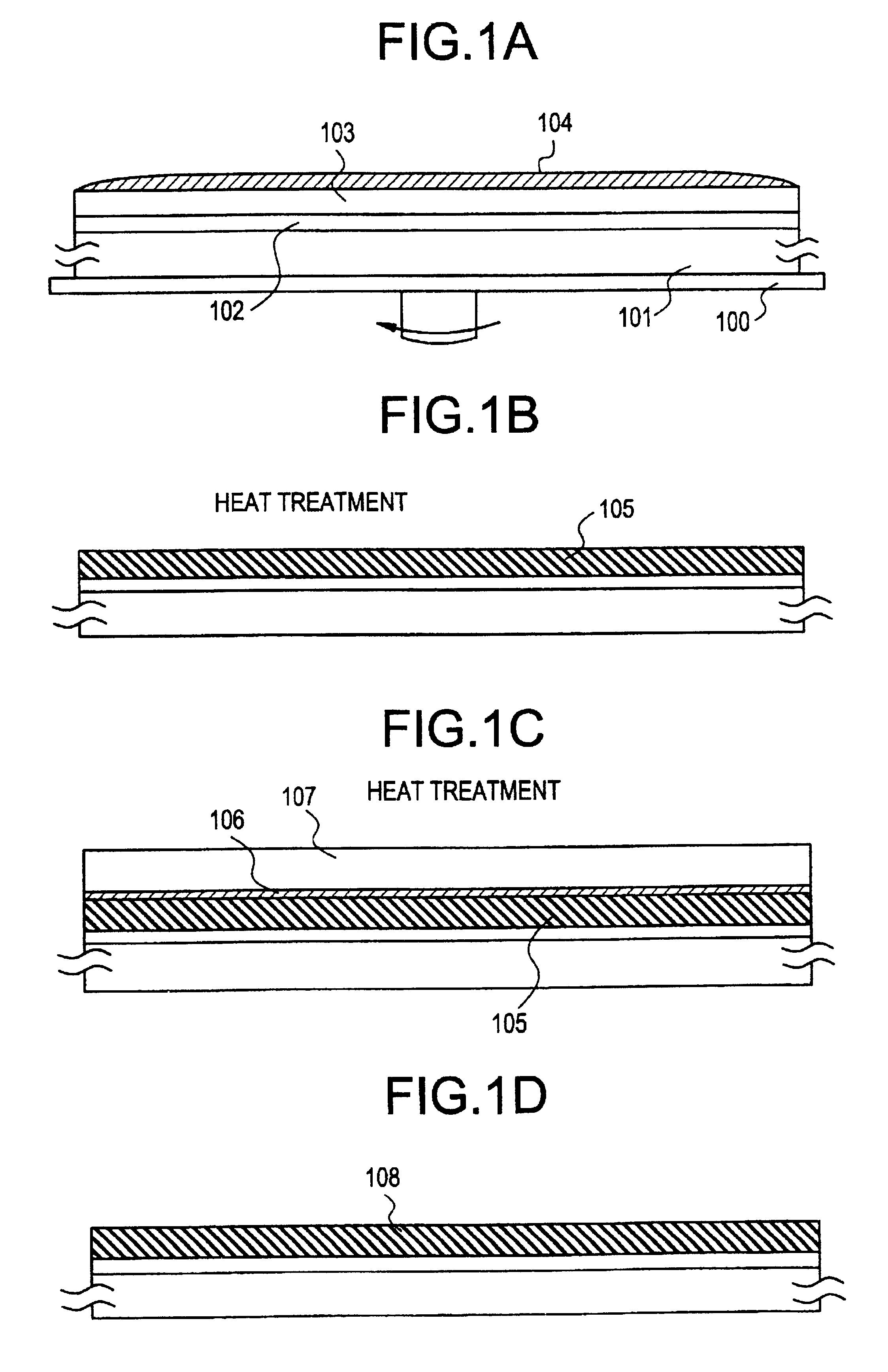
Embodiment 1 relates to a technology of dispersing a nickel element into an amorphous silicon film from a crystalline silicon film (allowing the amorphous silicon film to such the nickel element) to lower a density of the nickel element in the crystalline silicon film as a consequence, by forming an amorphous silicon film, introducing into the amorphous silicon film a metal film which promotes the crystallization of silicon film, forming an amorphous silicon film on a crystallized silicon film (crystalline silicon film) via an oxide film (silicon oxide film), followed by performing heat treatment again.

FIG. 1 shows a step of fabricating a crystalline silicon film described in this embodiment. In the beginning, on Corning 7059 glass substrate 101 (having a strain point of 593.degree. C.), a silicon oxide film 102 is formed to a thickness of 3000 .ANG. as a base film. The silicon oxide film 102 is intended to prevent impurities and alkaline ions from being dispersed into the semicondu...

embodiment 2

Embodiment 2 is characterized in that the step of heat treatment in the fabrication process in embodiment 1 is carried out by setting the conditions as follows; heating temperature is 550.degree. C., and heating duration is four hours. When the heat treatment step shown in FIG. 1(C) is carried out at 550.degree. C. for four hours, the amorphous silicon film denoted by 107 is crystallized with the action of the nickel element which is dispersed from the crystalline silicon film 105.

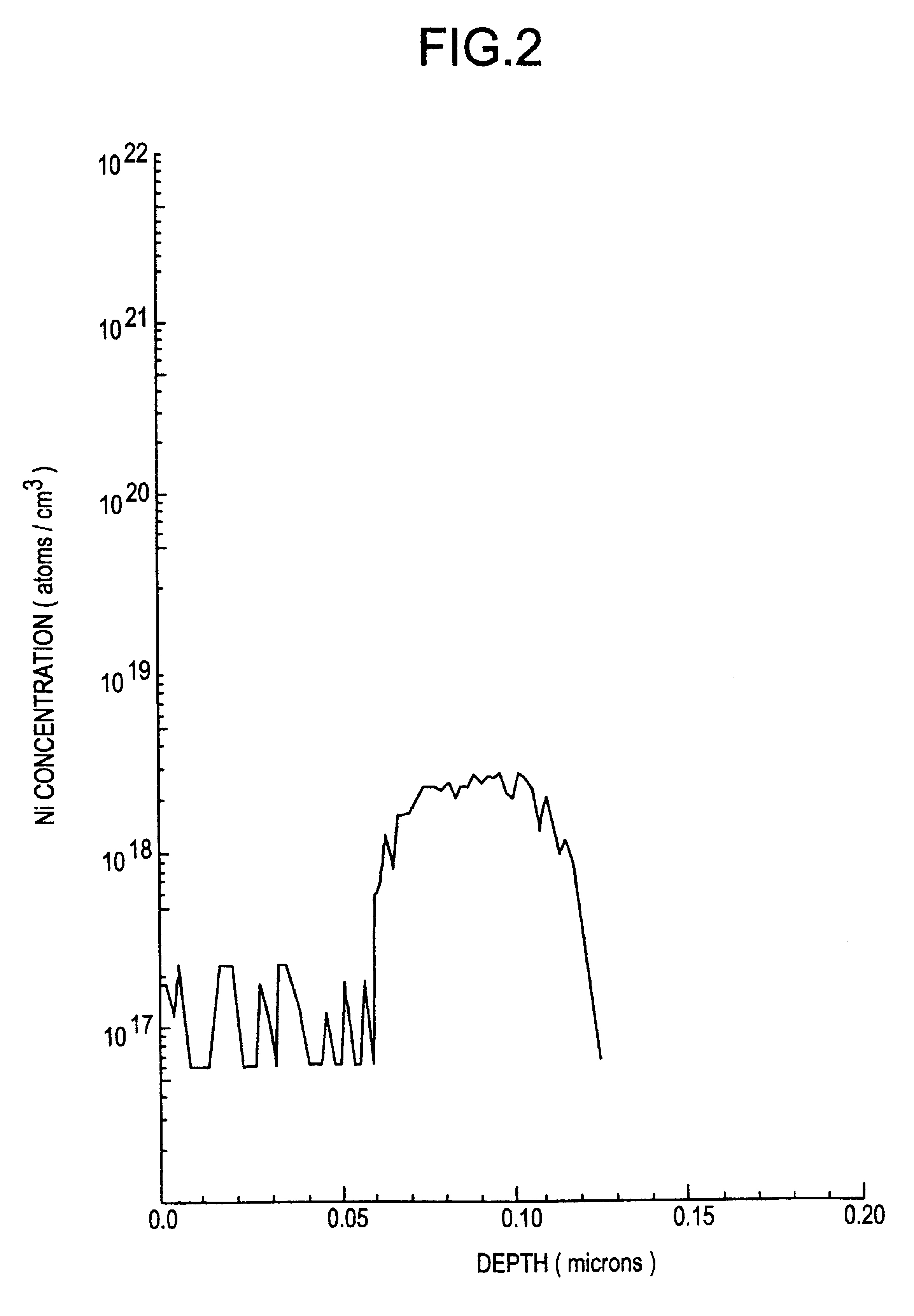
At this time, the crystalline advances in a direction of heading from the crystalline silicon film 105 to the amorphous silicon film 107 via the oxide film 106. As described above, the metal element which promotes the crystallization of silicon tends to be concentrated at the tip portion of the crystal growth. Consequently, an area where the nickel element is concentrated exist in the crystallized silicon film 107 (which is transformed into a crystalline film at this stage). Then naturally the density of n...

embodiment 3

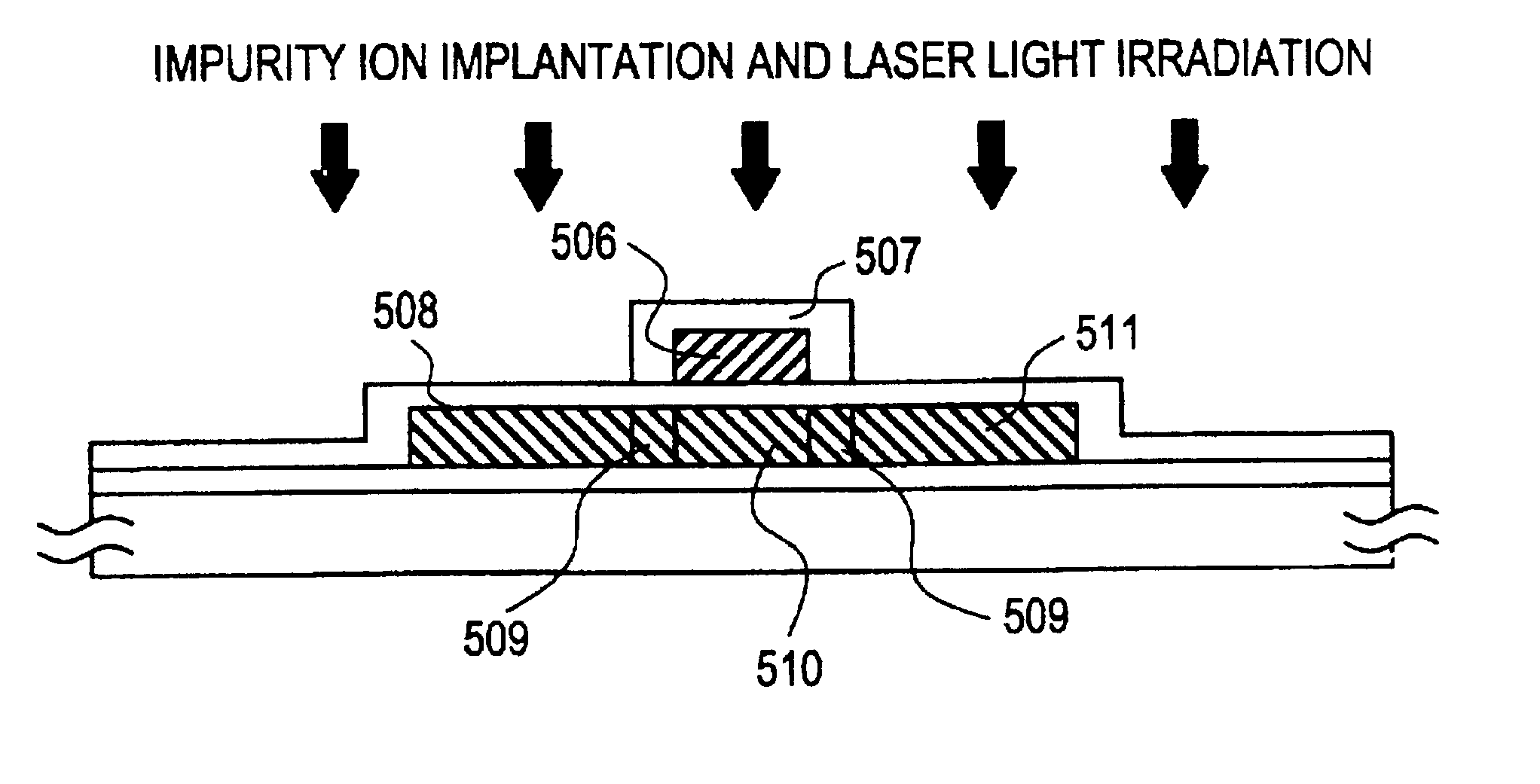
Embodiment 3 shows an example of fabricating a thin film transistor by using the crystalline silicon film which is obtained by the method for fabricating the silicon film shown in embodiments 1 and 2. Referring to FIG, 5, there is shown a method for fabricating the thin film transistor. In the beginning, a crystalline silicon film 503 is formed on the glass substrate 501 on which a base film 502 is formed by using a method shown in embodiments 1 and 2. (FIG. 5(A)) Subsequently, the crystalline silicon film 503 thus obtained is patterned to form an active layer of the thin film transistor as shown by reference numeral 504. Then a silicon oxide film 505 is formed to a thickness of 1000 .ANG. which functions as a gate insulating film by the plasma CVD and the low pressure thermal CVD. (FIG. 5(B))

Then an aluminum film containing scandium is formed to a thickness of 6000 .ANG. followed by patterning the film to form a gate electrode denoted by reference numeral 506. Further, in the elect...


PUM

PropertyMeasurementUnit
Densityaaaaaaaaaa
Crystallization enthalpyaaaaaaaaaa
Semiconductor propertiesaaaaaaaaaa

Abstract

An object of the present invention is to provide a technology of reducing a nickel element in the silicon film which is crystallized by using nickel. An extremely small amount of nickel is introduced into an amorphous silicon film which is formed on the glass substrate. Then this amorphous silicon film is crystallized by heating. At this time, the nickel element remains in the crystallized silicon film. Then an amorphous silicon film is formed on the surface of the silicon film crystallized with the action of nickel. Then the amorphous silicon film is further heat treated. By carrying out this heat treatment, the nickel element is dispersed from the crystallized silicon film into the amorphous silicon film with the result that the nickel density in the crystallized silicon film is lowered.

Description

BACKGROUND OF THE INVENTION1. Field of the InventionThe present invention relates to a method for forming a silicon semiconductor thin film which has a crystallinity and is formed on a substrate having an insulation surface of a glass substrate or the like.2. Description of the Related ArtIn recent years, attention is paid on a technology for constructing a thin film transistor by using a silicon thin film which is formed on a glass substrate. This thin film transistor is primarily used in an active matrix type liquid crystal electro-optical device and other thin film integrated circuits. The liquid crystal electro-optical device changes optical characteristics of a liquid crystal thereby displaying an image by charging a liquid crystal into a pair of glass substrates and applying an electric field.In particular, the active matrix type liquid crystal display device using a thin film transistor is characterized in that the thin film transistor is arranged in each pixel, an electric c...

Claims


Application Information

Patent Timeline
IPC IPC(8): H01L29/786H01L21/20H01L29/66H01L21/02
CPCH01L29/78675C03C17/3482C03C2218/152C03C2218/153H01L21/02422H01L21/02488H01L21/02532H01L21/02505H01L21/02675H01L21/0245H01L21/02672
Inventor YAMAZAKI, SHUNPEIOHTANI, HISASHIMIYANAGA, AKIHARUTERAMOTO, SATOSHI
Owner SEMICON ENERGY LAB CO LTD
Why Eureka
Try Eureka