Semiconductor yield management system and method

a technology of yield management and semiconductor, applied in semiconductor/solid-state device testing/measurement, instruments, computing, etc., can solve the problems of reducing the yield of the final semiconductor product, affecting the yield of the semiconductor, and the complexity of the semiconductor manufacturing process, so as to achieve easy interpretation and understanding, and easy use

Inactive Publication Date: 2011-06-21
RUDOLPH TECHNOLOGIES INC
View PDF5 Cites 2 Cited by
  • Summary
  • Abstract
  • Description
  • Claims
  • Application Information

AI Technical Summary

Benefits of technology

[0006]The yield management system and method in accordance with the invention may provide many advantages over conventional methods and systems which make the yield management system and method more useful to semiconductor device manufacturers. In particular, the system may be fully automated and easy to use so that no extra training is necessary to make use of the yield management system. In addition, the system handles both continuous (e.g., temperature) and categorical (e.g., Lot 1, Lot 2, etc.) variables. The system also automatically handles missing data during a pre-processing step. The system can rapidly search through hundreds of yield parameters and generate an output indicating the one or more key yield factors / parameters. The system generates an output (a decision tree) that is easy to interpret and understand. The system is also very flexible in that it permits prior yield parameter knowledge (from users) to be easily incorporated into the building of the model in accordance with the invention. Unlike conventional systems, if there is more than one yield factor / parameter affecting the yield of the process, the system can identify all of the parameters / factors simultaneously so that the multiple factors are identified during a single pass through the yield data.

Problems solved by technology

The semiconductor manufacturing process is extremely complicated since it involves hundreds of processing steps.
A mistake or small error at any of the process steps or tool specifications may cause lower yield in the final semiconductor product, wherein yield may be defined as the number of functional devices produced by the process as compared to the theoretical number of devices that could be produced assuming no bad devices.
Improving yield is a critical problem in the semiconductor industry and has a direct economic impact to the semiconductor industry.
In particular, the database technology has far outpaced the yield management ability when using conventional statistical methods to interpret and relate yield to major yield factors.
Current conventional yield management systems have a number of limitations and disadvantages which make them less desirable to the semiconductor industry.
For example, the conventional systems may require some manual processing which slows the analysis and makes it susceptible to human error.
In addition, these conventional systems may not handle both continuous and categorical yield management variables.
Some conventional systems cannot handle missing data elements and do not permit rapid searching through hundreds of yield parameters to identify key yield factors.
Some conventional systems output data that is difficult to understand or interpret even by knowledgeable semiconductor yield management people.
In addition, the conventional systems typically process each yield parameter separately, which is time consuming and cumbersome and cannot identify more than one parameter at a time.

Method used


Image

  • Semiconductor yield management system and method
  • Semiconductor yield management system and method
  • Semiconductor yield management system and method

Examples


Embodiment Construction

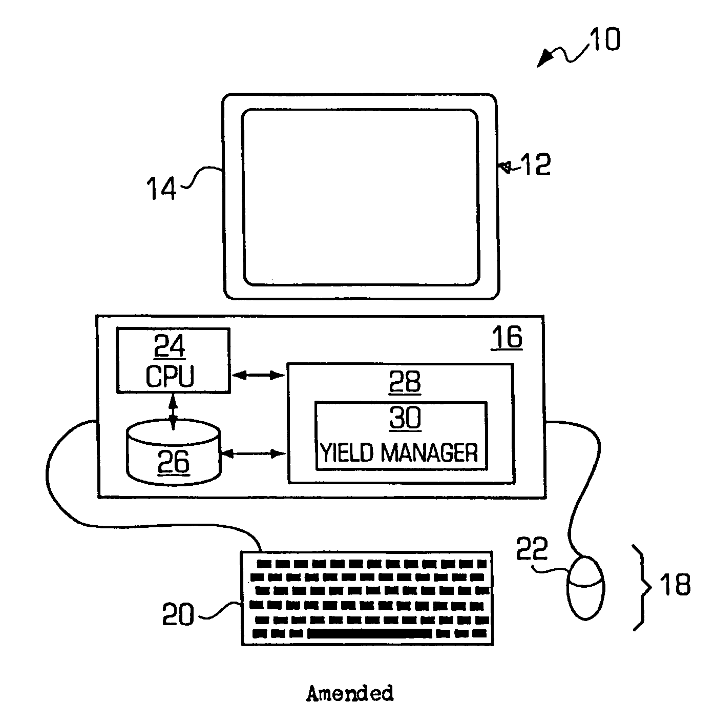
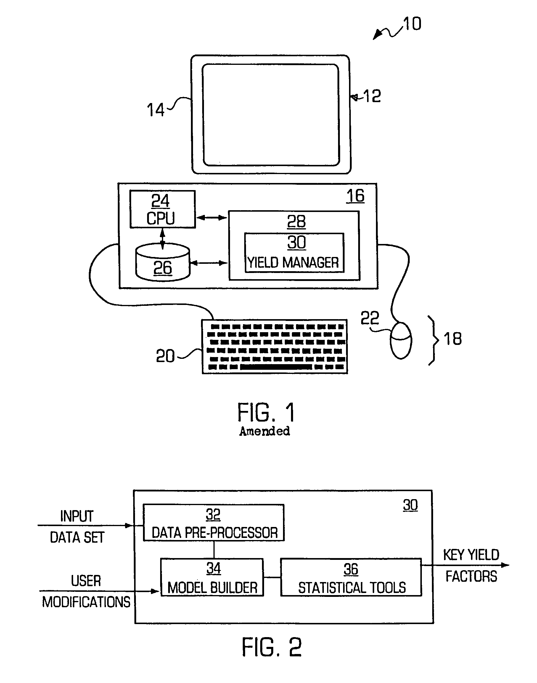
[0017]The invention is particularly applicable to a computer-implemented software-based yield management system and it is in this context that the invention will be described. It will be appreciated, however, that the system and method in accordance with the invention has greater utility since it may be implemented in hardware or may incorporate other modules or functionality not described herein.

[0018]FIG. 1 is a block diagram illustrating an example of a yield management system 10 in accordance with the invention implemented on a personal computer 12. In particular, the personal computer may include a display unit 14, that may be a cathode ray tube (CRT), a liquid crystal display or the like, a processing unit 16 and one or more input / output devices 18 that permit a user to interact with the software application being executed by the personal computer. In this example, the input / output devices may include a keyboard 20 and a mouse 22, but may also include other peripheral devices ...


PUM


Abstract

A system and method for yield management is disclosed wherein a data set containing one or more prediction variable values and one or more response values is input into the system. The system can pre-process the input data set to remove prediction variables with missing values and data sets with missing values. The pre-processed data can then be used to generate a model that may be a decision tree. The system can accept user input to modify the generated model. Once the model is complete, one or more statistical analysis tools can be used to analyze the data and generate a list of the key yield factors for the particular data set.

Description

BACKGROUND OF THE INVENTION[0001]This invention relates generally to a system and method for managing a semiconductor process and in particular to a system and method for managing yield in a semiconductor process.[0002]The semiconductor industry is continually pushing toward smaller and smaller geometries of the semiconductor devices being produced since smaller devices generate less heat and operate at a higher speed than larger devices. Currently, a single chip may contain over one billion patterns. The semiconductor manufacturing process is extremely complicated since it involves hundreds of processing steps. A mistake or small error at any of the process steps or tool specifications may cause lower yield in the final semiconductor product, wherein yield may be defined as the number of functional devices produced by the process as compared to the theoretical number of devices that could be produced assuming no bad devices. Improving yield is a critical problem in the semiconducto...

Claims


Application Information

Patent Timeline
Patent Type & Authority Patents(United States)
IPC IPC(8): G06F19/00H01L21/66
CPCH01L22/20
Inventor WANG, WEIDONGBUCKHEIT, JONATHAN B.BUDD, DAVID W.
Owner RUDOLPH TECHNOLOGIES INC
Why Eureka
Try Eureka